Exposure method and tool

a technology applied in the field of exposure method and exposure tool, can solve the problems of pattern defect, low yield, and low mask lifetime, and achieve the effects of avoiding significant resolution loss, avoiding loss of resolution, and simple construction

Inactive Publication Date: 2009-04-16
EXITECH
View PDF1 Cites 13 Cited by
  • Summary
  • Abstract
  • Description
  • Claims
  • Application Information

AI Technical Summary

Benefits of technology

[0070]As with projection SIS exposure, for proximity SIS exposure it is also necessary to use beam shaping apertures to avoid band overlap exposure uniformity problems and moving blades to define the FPD boundaries correctly. Such devices can be incorporated into the floating optics head immediately above the mask without significant difficulty. It is also possible to combine the functions of the pattern forming mask and the beam shaping mask onto a single mask device if appropriate. Such an arrangement leads to a simpler construction within the floating optics head.
[0071]Illumination of the proximity mask must be performed with some care to avoid loss of resolution. If the gap between mask and resist is maintained at about 50 μm to 100 μm it is necessary that the illuminating radiation is collimated to within a range of angles less than 10 milliradians to avoid significant loss of resolution. It is also necessary to ensure that the illumination is uniform across the mask in the direction perpendicular to the scan direction to ensure uniformity of exposure across the scan bands. Illumination uniformity in the beam direction parallel to the scan direction is not critical since any non-uniformities in this direction are averaged by the scan motion.

Problems solved by technology

To allow the passage of the UV radiation (typically at a wavelength of 365 nm (i-line)) the mask has to be made of UV transmitting fused silica Such proximity exposure technology is not overly complex in terms of equipment requirements but, because of the gap and uniformity control difficulties, variations in the resist pattern can be large, leading to defects in the pattern (i.e. yield is low).
Mask lifetime is also low as constant movement and handling cause rapid contamination.
However as FPD displays get larger e.g. 40 inch (1000 mm) and greater diagonal and especially for PDPs where sizes over 60 inch (1500 mm) and greater diagonal or more are needed the provision of suitable one-times masks is difficult and costly.

Method used


Image

  • Exposure method and tool
  • Exposure method and tool
  • Exposure method and tool

Examples


Embodiment Construction

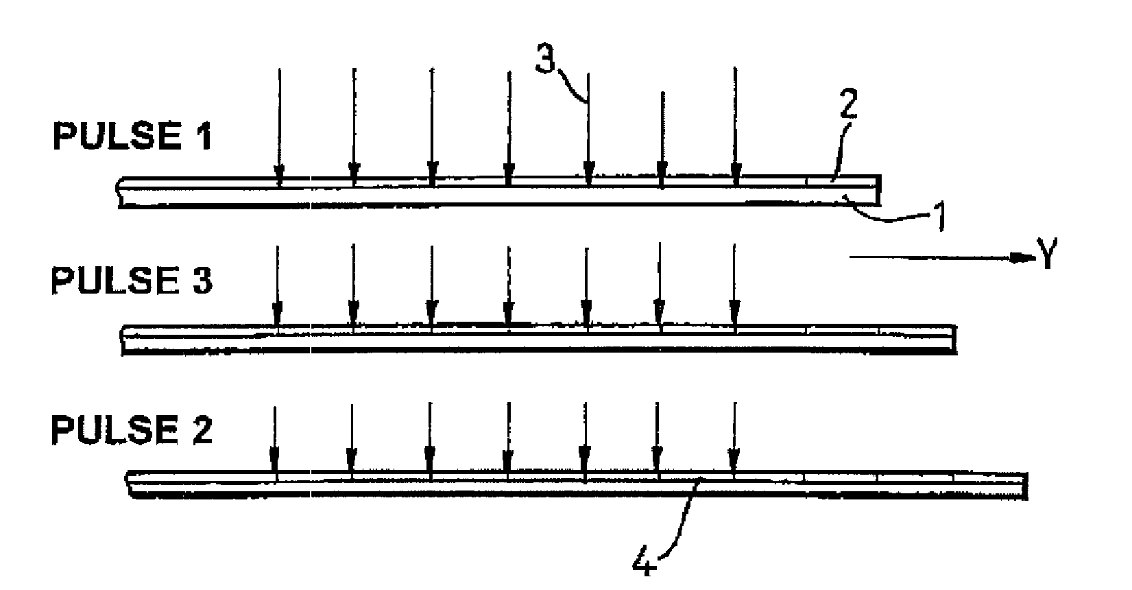
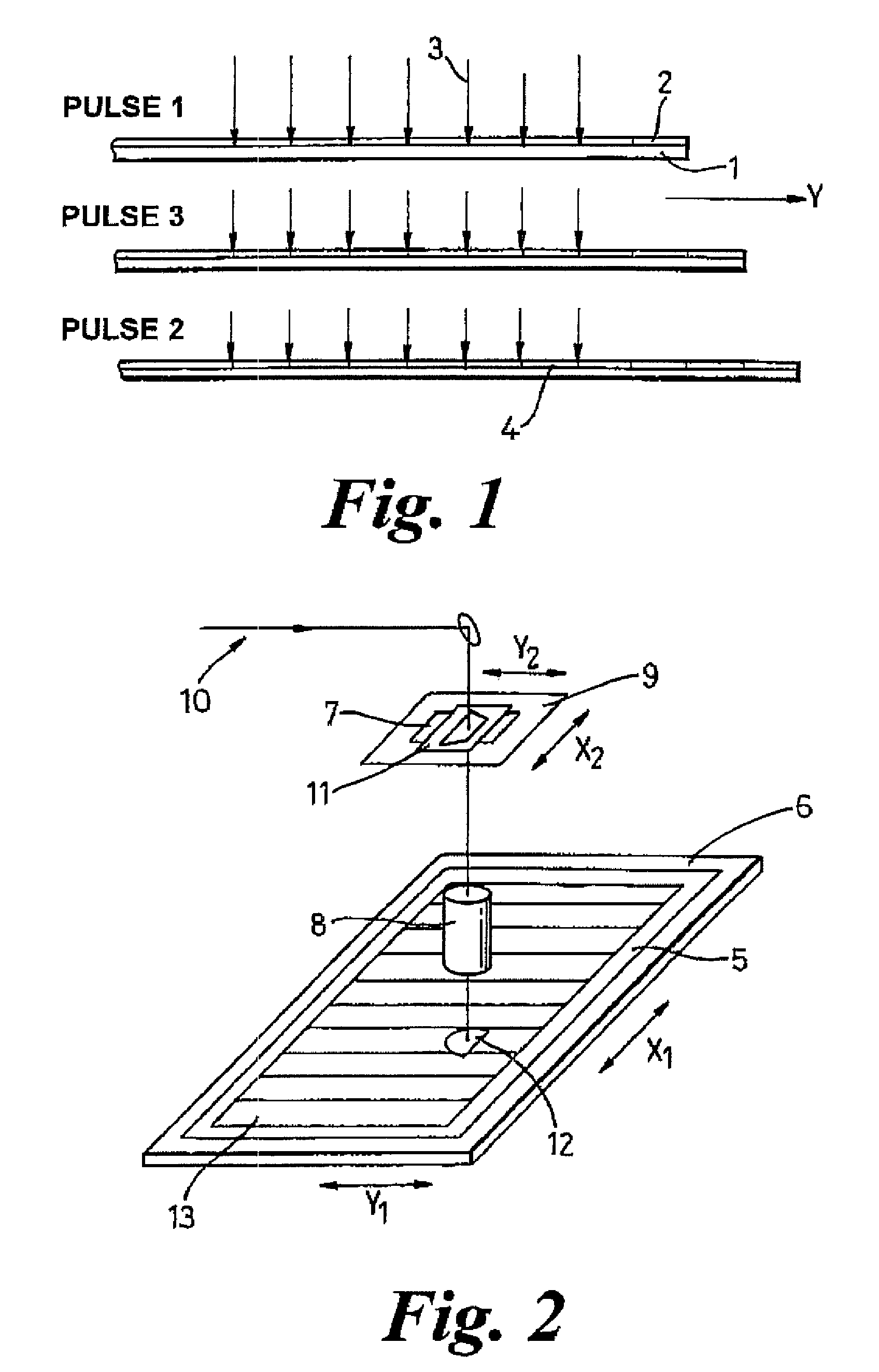
[0082]FIG. 1 shows the principle of the SIS exposure method. A substrate 1 coated with a photo resist layer 2 is moved progressively under the exposing pulsed radiation beam 3 in direction Y. The beam creates an image on the resist that corresponds to the required pixel or cell structure of the FPD. In the figure the image is shown to contain 6 pixel cells in the direction in which the substrate is moving. Each pulse of radiation hence exposes a band of resist that is 6 cells wide. Between laser pulses the substrate moves exactly 1 cell pitch so that the next pulse creates a pattern that exactly overlaps the first but is displaced by 1 cell pitch. In the figure shown where the beam is 6 cells wide each area of resist receives 6 pulses of radiation and then moves from the beam.

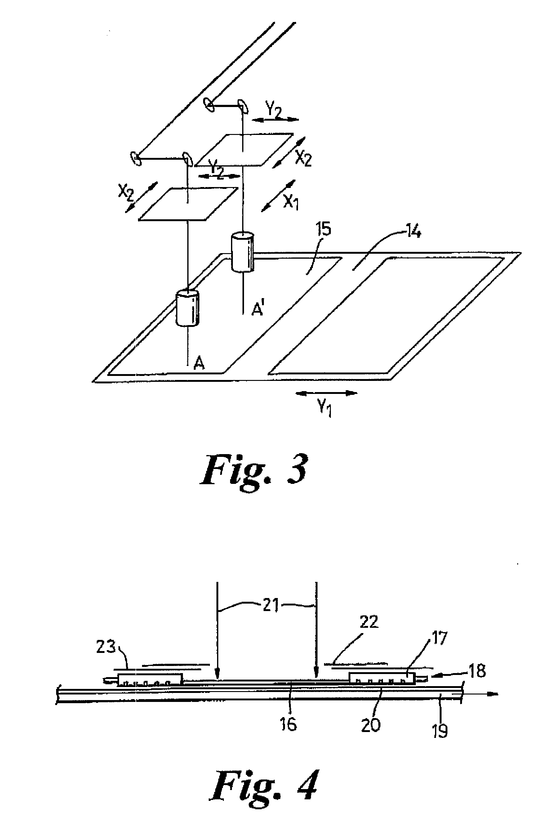
[0083]FIG. 2 shows a possible geometry for an SIS projection exposure tool. A glass substrate 5, coated with an indium-tin oxide (‘ITO’) or tin oxide (‘SnO2’) layer and a suitable resist layer, which is to be u...


PUM

PropertyMeasurementUnit
wavelengthaaaaaaaaaa
diameteraaaaaaaaaa
sizesaaaaaaaaaa

Abstract

A method for forming a regularly repeating pattern on to a substrate comprising the steps of: applying a resist on a surface of a substrate to be processed; imprinting on the applied resist a pattern formed by exposing it to a beam of ultra violet (‘UV’) light, which has been caused to pass through a suitable mask delineating the pattern and then trough a focusing lens on to the resist, so as to cause chemical changes in the resist which makes it more or less soluble in a suitable developer solution; the imprinting step being carried out: in a repetitive series of discrete exposure steps using a mask held stationery with respect to the beam and the lens that represents only a small area of the total area of the substrate and using a single short pulse of UV radiation at each step to illuminate the mask, the radiation pulse having such an energy density at the substrate that it is below the threshold value for ablation of the resist; and the series of discrete exposure steps being repeated over the full area of the surface of a substrate, to give a full structure comprising a plurality of pixels, by moving the substrate in a direction parallel to one axis of the structure to be formed on the substrate and activating the pulsed mask illumination light source at the instant that the substrate has moved over a distance equivalent to a complete number of periods of the repeating pattern on the substrate; treating the exposed resist with a developer to cause either exposed regions (for positive resists) or unexposed regions (for negative resists) to be dissolved and subsequently washed away by the developer solution to reveal the pattern formed by the remaining resist; treating the substrate with a suitable chemical etching solution, reactive plasma or abrasive particles that removes the substrate in resist free areas; and removing remaining resist from the substrate with a suitable solvent to leave a finished patterned substrate.
The invention further comprises a scanning exposure tool for carrying out the method as aforesaid.

Description

[0001]This application is a national stage completion of PCT / GB2006 / 000305 filed Jan. 30, 2006 which claims priority from British Application Serial No. 0501793.4 filed Jan. 28, 2005.FIELD OF THE INVENTION[0002]This invention relates to an exposure method and a tool. It is particularly concerned with the field of photo-resist exposure for the processing of large area glass substrates used in the manufacture of flat panel displays.BACKGROUND OF THE INVENTION[0003]The manufacture of a flat panel display (‘FPD’) requires multiple process steps which include lithographic pattern transfer from a mask using photo-resists.[0004]A method is known for forming a pattern on a substrate involving the steps of:[0005](1) applying a resist on a surface of a substrate to be processed;[0006](2) imprinting on the applied resist a pattern formed by exposing it to ultra violet (‘UV’) light, which has been caused to pass through a suitable mask delineating the pattern, so as to cause chemical changes in...

Claims


Application Information

Patent Timeline
Patent Type & Authority Applications(United States)
IPC IPC(8): G03F7/20G03B27/42
CPCG03F7/70041G03F7/70283G03F7/70358G03F7/70791G03F7/70466G03F7/70475G03F7/70725G03F7/70425
Inventor SYKES, NEILALLOTT, RICHARD
Owner EXITECH
Why Eureka
Try Eureka