

Method for manufacturing semiconductor device, semiconductor device, and electronic appliance
- Summary
- Abstract
- Description
- Claims
- Application Information
AI Technical Summary
Benefits of technology
Problems solved by technology
Method used
Image

Examples
embodiment mode 1
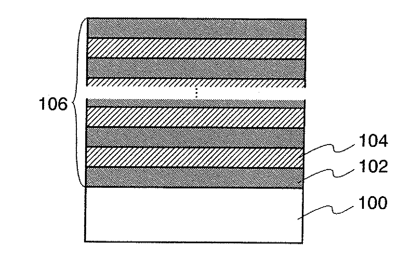
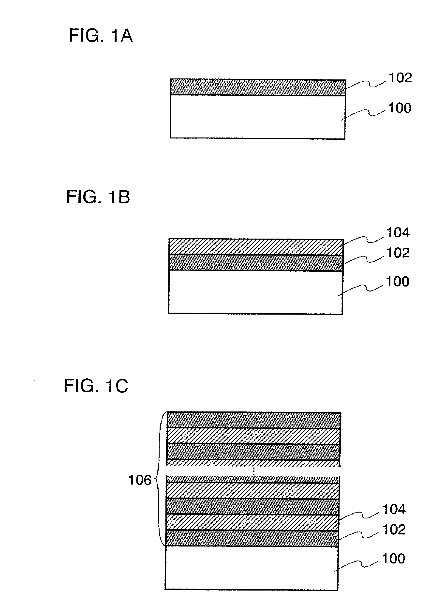
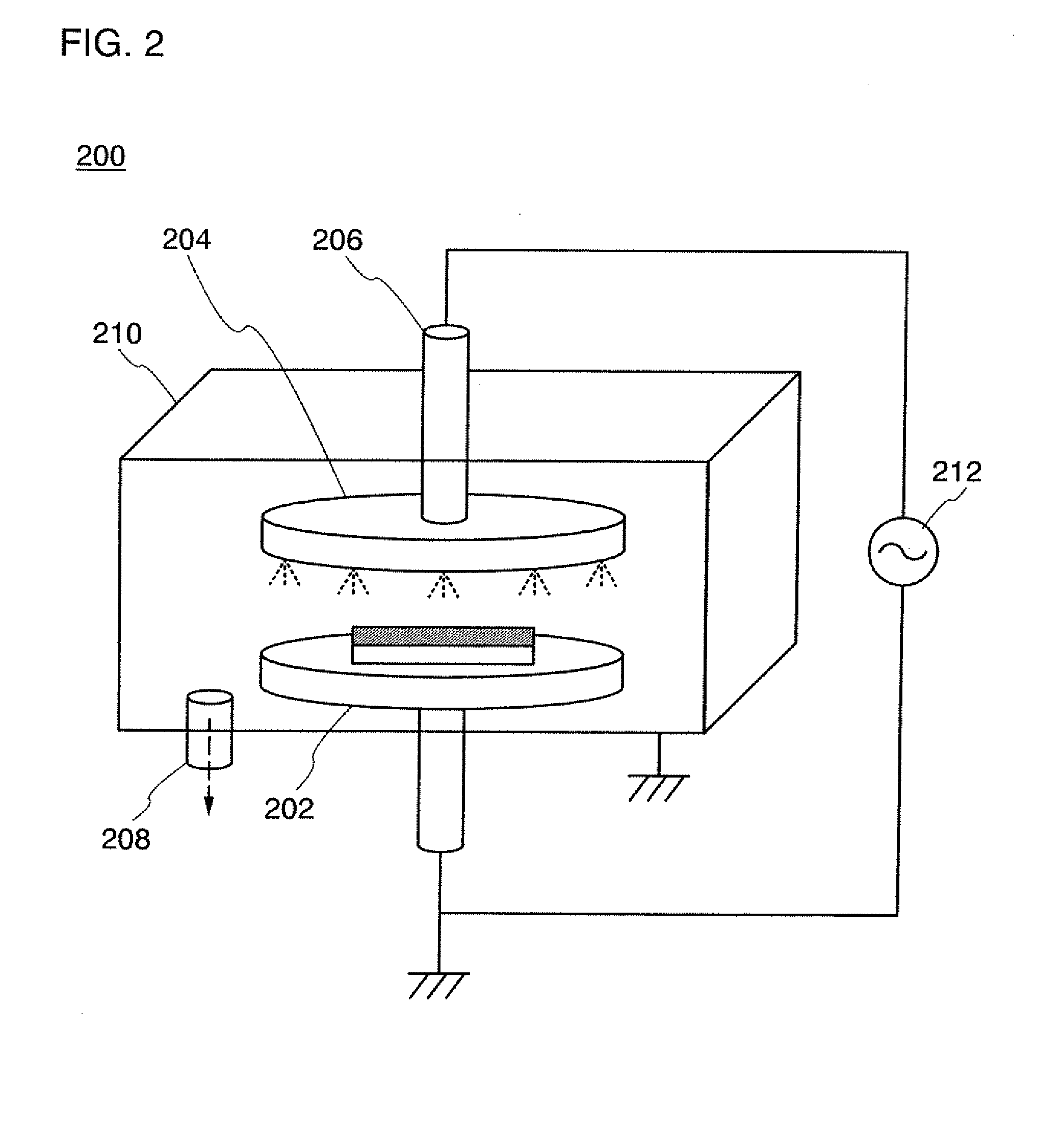
[0048]In this embodiment mode, an insulating layer according to the present invention will be described with reference to FIGS. 1A to 1C, FIG. 2, FIGS. 3A to 3C, FIGS. 4A and 4B, FIGS. 5A and 5B, and FIGS. 6A and 6B.
[0049]First, an insulator 102 containing nitrogen is formed on a surface of an object to be processed 100 (also referred to as a surface to be processed) (see FIG. 1A). The object to be processed 100 is not particularly limited and, for example, may be a substrate used for manufacturing a semiconductor device. As the substrate, a non-alkali glass substrate such as a barium borosilicate glass substrate, an aluminoborosilicate glass substrate, or an aluminosilicate glass substrate, a ceramic substrate, or the like can be used. Alternatively, a plastic substrate or the like may be used as long as it resists heat. Still alternatively, a metal substrate such as a stainless steel alloy, a single crystal semiconductor substrate, a quartz substrate, or the like may be used. The ...
embodiment mode 2
[0077]In this embodiment mode, an example of a semiconductor device using an insulating layer of the present invention will be described with reference to FIGS. 7A to 7D, FIGS. 8A to 8C, FIGS. 9A to 9D, FIGS. 10A to 10C, and FIGS. 11A to 11C.
[0078]Here, a semiconductor device using a so-called SOI (silicon on insulator) substrate will be described. An SOI substrate is provided with a thin single crystal semiconductor layer on the insulating surface thereof. By using this, a semiconductor device with high performance can be obtained. In this embodiment mode, used is an SOI substrate obtained by providing a single crystal semiconductor layer over a base substrate using a glass material or the like with an insulating layer serving as a bonding layer interposed therebetween. Note that an SOI substrate used in this embodiment mode is obtained by separating a single crystal semiconductor substrate at region, into which ions are introduced, to form a single crystal semiconductor layer over...
embodiment mode 3
[0136]This embodiment mode will describe an example of a manufacturing method of a liquid crystal display device as an example of a semiconductor device using an insulating layer of the present invention, with reference to FIGS. 12A to 12D, FIGS. 13A to 13C, FIGS. 14A to 14C, and FIGS. 15A and 15B.
[0137]First, a single crystal semiconductor layer is formed over a substrate having an insulating surface by the method described in Embodiment Mode 1, or the like (see FIG. 12A). Here, the structure in which an insulating layer 1202 serving as a barrier layer, an insulating layer 1204 serving as a bonding layer, and a single crystal semiconductor layer 1206 are sequentially provided over a substrate 1200 having an insulating surface is described; however, the present invention is not limited thereto. Next, the single crystal semiconductor layer 1206 and the insulating layer 1204 are patterned into a desired shape to form island-shaped single crystal semiconductor layers.
[0138]As to an etc...
PUM
| Property | Measurement | Unit |
|---|---|---|
| Thickness | aaaaa | aaaaa |
| Concentration | aaaaa | aaaaa |
| aaaaa | aaaaa |
Abstract
Description
Claims
Application Information