Friction Control in Apparatus Having Wide Bandgap Semiconductors

Inactive Publication Date: 2009-04-30
HIRD JONATHAN +3
View PDF3 Cites 6 Cited by
  • Summary
  • Abstract
  • Description
  • Claims
  • Application Information

AI Technical Summary

Benefits of technology

[0010]According to one aspect of the invention, there is provided apparatus comprising a wide bandgap semiconductor and a conductor having an interface with the semiconduct

Problems solved by technology

Such semiconductors may not easily form ohmic contacts and do not

Method used


Image

  • Friction Control in Apparatus Having Wide Bandgap Semiconductors
  • Friction Control in Apparatus Having Wide Bandgap Semiconductors
  • Friction Control in Apparatus Having Wide Bandgap Semiconductors

Examples


Embodiment Construction

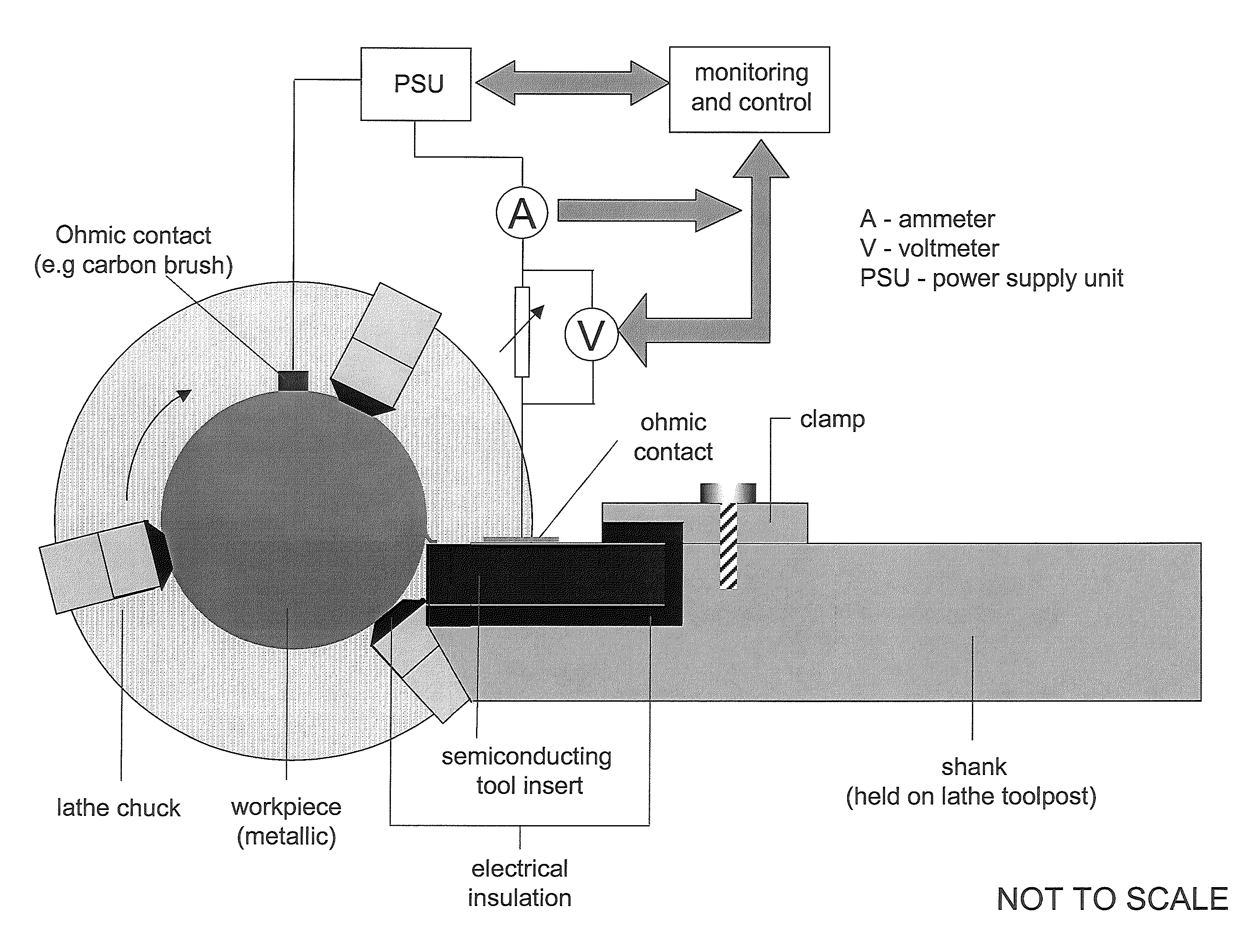
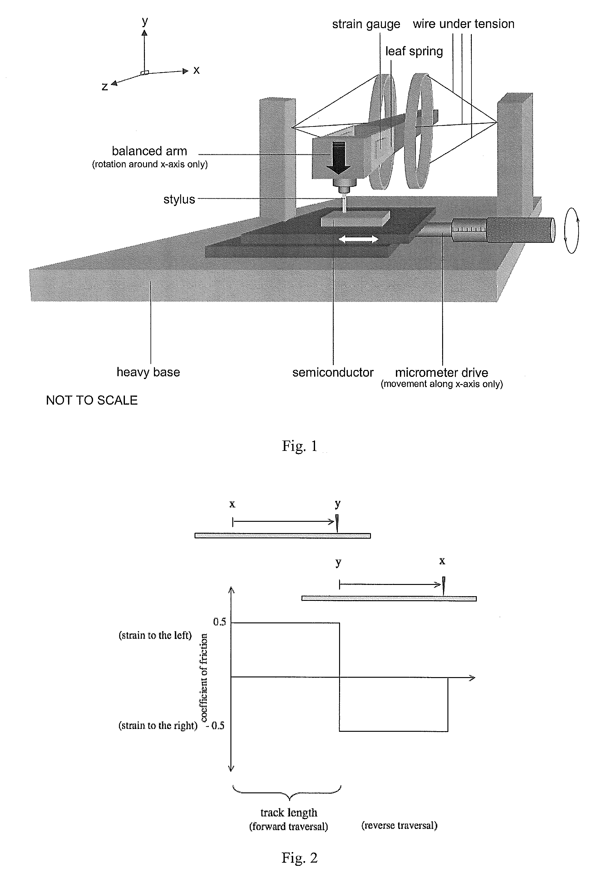
[0031]FIG. 1 is a schematic of apparatus demonstrating the principles of the invention. The apparatus is similar in operation to that described by I. P Hayward & J. E. Field ‘A computer-controlled friction measuring apparatus’ (J. Phys E: Sci. Instrum. 21 1988 p. 753-756). A semiconducting sample, e.g. p-type semiconducting diamond (bandgap≈3.6 eV), is mounted on an insulating block. The block is mounted on a motor-driven micrometer stage which is drive back and forth under a stylus. The stylus is a conductor and may be metallic, e.g. steel, aluminium (Al), copper (Cu), iron (Fe), nickel (Ni), molybdenum (Mo), platinum (Pt) or tungsten (W) or a non-metallic conductor, e.g. graphite from a pencil or it may be a standard semiconductor, e.g. silicon (Si) or germanium (Ge). The stylus is mounted by means of two leaf springs to an arm which is held rigid save for being allowed to rotate around the x-axis. Two strain gauges are attached to either side of each leaf spring. These are wired ...


PUM


Abstract

Apparatus comprising, in use, a wide bandgap semiconductor, a conductor which is moveable relative to the semiconductor and means for applying a potential across the junction between a conductor and semiconductor to control the friction generated by the relative movement between the semiconductor and the conductor. A method of controlling friction between a wide bandgap semiconductor and conductor which are moveable relative to each other comprising applying a potential across the junction between the semiconductor and the conductor.

Description

RELATED APPLICATIONS[0001]The present invention claims priority from British Patent Application No. GB0721304.4, filed 31 Oct. 2007.FIELD OF THE INVENTION[0002]The invention relates to friction control in any tribological applications having wide bandgap semiconductors in sliding contact with conductors, for example tool machining apparatus.BACKGROUND TO THE INVENTION[0003]Aside from its role as the world's most sought after gemstone, diamond remains one of the most prominently used abrasives and tool materials. Indeed, the market size of the diamond tool and abrasives market dwarves that of its gemstone counterpart. Emerging technologies utilising some of the more extreme properties of diamond such as its thermal conductivity, very low friction coefficient when sliding against itself, hardness and semiconducting properties are set to widen this gap further as markets open and are developed further.[0004]The Achilles heel of diamond, however, is a thermo-chemical reaction that occur...

Claims


Application Information

Patent Timeline
IPC IPC(8): H01L29/15B24B7/00B24B49/00B24B37/04
CPCB24B49/14B24B37/042
Inventor HIRD, JONATHANCHAKRAVARTY, AVIKCHAKRAVARTY, SATYENDRACHAKRAVARTY, CHHAYA
Owner HIRD JONATHAN
Why Eureka
Try Eureka