Method for manufacturing soi substrate

a technology substrate, which is applied in the direction of basic electric elements, electrical apparatus, semiconductor devices, etc., can solve the problems of defective bonding, surface of silicon nitride film, defective bonding, etc., and achieve the effect of simplifying the process and suppressing the occurrence of defective bonding between the base substrate and the semiconductor substra

Inactive Publication Date: 2009-04-30
SEMICON ENERGY LAB CO LTD
View PDF12 Cites 28 Cited by
  • Summary
  • Abstract
  • Description
  • Claims
  • Application Information

AI Technical Summary

Benefits of technology

[0021]According to the present invention, in manufacturing an SOI substrate, the occurrence of defective bonding between a base substrate and a semiconductor substrate can be suppressed even when a silicon nitride film or the like is used as a bonding layer. In addition, according to the present invention, in manufacturing an SOI substrate, simplification of a process can be achieved.

Problems solved by technology

However, in the case where a silicon nitride film or the like is formed by a CVD method or the like, the obtained film has an uneven surface or the like; thus, in the case where the silicon nitride film or the like is used as a bonding layer, defective bonding may occur in bonding a base substrate and a single crystal semiconductor substrate to each other.
In addition, in the case where ions are added to a single crystal silicon substrate through a silicon nitride film or the like having an uneven surface, the surface of the silicon nitride film or the like is roughened as well as being uneven; thus, defective bonding may occur with high possibility in bonding a base substrate and a single crystal silicon substrate to each other.
As a result, a single crystal silicon layer obtained over a base substrate may be defective, and an element such as a transistor that is manufactured using the single crystal silicon layer may have insufficient characteristics.
This causes problems such as an increase in the number of steps and a restriction on a process.
In manufacturing an SOI substrate, a cost reduction by simplification of a process or the like is important because a single crystal silicon substrate used is expensive.
Moreover, as the number of insulating films stacked increases, reliability may decrease; for example, defective bonding may occur due to dust or an impurity which is generated with an increase in the number of steps.

Method used


Image

  • Method for manufacturing soi substrate
  • Method for manufacturing soi substrate
  • Method for manufacturing soi substrate

Examples


embodiment mode 1

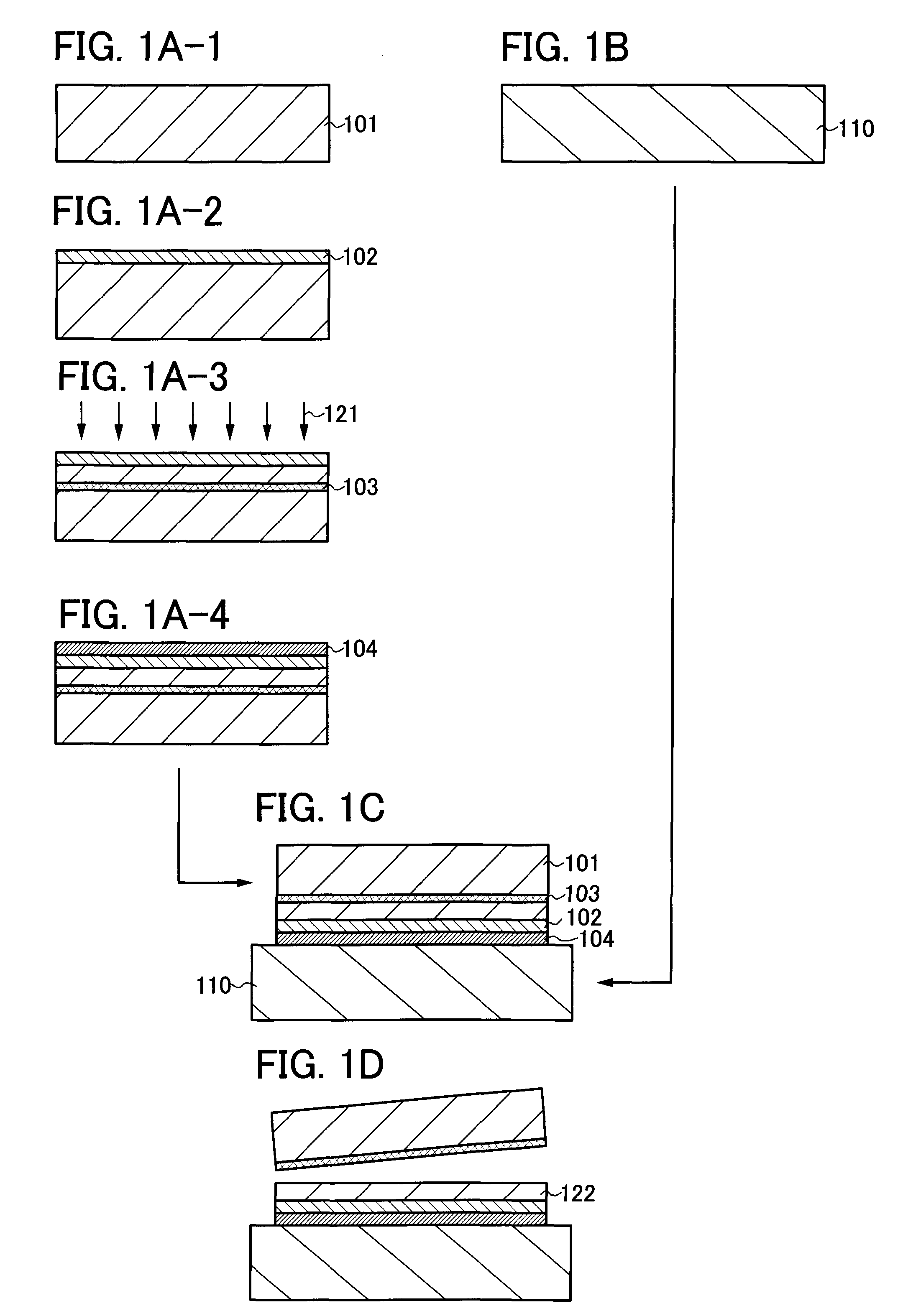
[0041]In this embodiment mode, an example of a method for manufacturing an SOI substrate of the present invention is described with reference to drawings.

[0042]First, a semiconductor substrate 101 is prepared (see FIG 1A-1).

[0043]As the semiconductor substrate 101, a commercially available semiconductor substrate can be used. For example, a single crystal silicon substrate, a single crystal germanium substrate, or a compound semiconductor substrate of gallium arsenide, indium phosphide, or the like can be used. Typical examples of commercially available silicon substrates are circular silicon substrates which are 5 inches (125 mm) in diameter, 6 inches (150 mm) in diameter, 8 inches (200 mm) in diameter, and 12 inches (300 mm) in diameter. Note that the shape is not limited to a circular shape, and a silicon substrate processed into a rectangular shape or the like can also be used.

[0044]Next, an insulating film 102 is formed over a surface of the semiconductor substrate 101 (see FIG...

embodiment mode 2

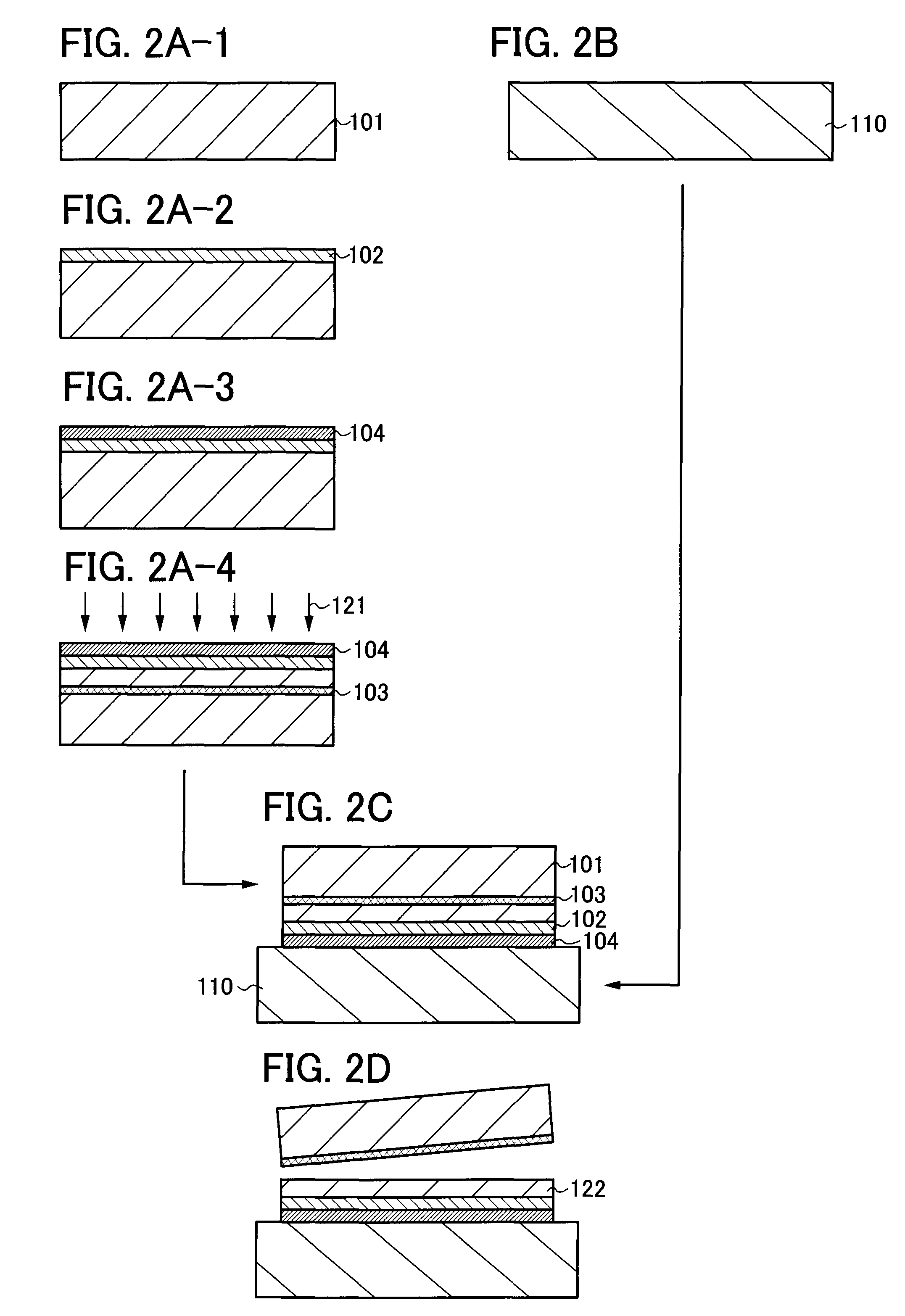
[0088]In this embodiment mode, a method for manufacturing an SOI substrate, which is different from that in the above-described embodiment mode, is described with reference to drawings. Specifically, a case is described in which a base substrate provided with a nitrogen-containing layer over its surface and a semiconductor substrate provided with an insulating film are bonded together.

[0089]First, a semiconductor substrate 101 is prepared (see FIG. 4A-1), and an insulating film 202 is formed over a surface of the semiconductor substrate 101 (see FIG. 4A-2).

[0090]In this embodiment mode, the insulating film 202 functions as a bonding layer to a base substrate. The insulating film 202 can be a silicon oxide film (SiOx) or a silicon oxynitride film (SiOxNy) (x>y) formed by a CVD method, a sputtering method, or the like. Alternatively, the insulating film 202 may be an insulating film (such as a silicon oxide film) formed by thermal oxidation of a surface of the semiconductor substrate ...

embodiment mode 3

[0108]In this embodiment mode, a method for manufacturing a semiconductor device using the SOI substrate manufactured in either one of the above-described embodiment modes is described.

[0109]First, as a method for manufacturing a semiconductor device, a method for manufacturing an n-channel thin film transistor and a p-channel thin film transistor is described with reference to FIGS. 5A to 5D and 6A to 6C. By combining a plurality of thin film transistors (TFTs), various types of semiconductor devices can be formed.

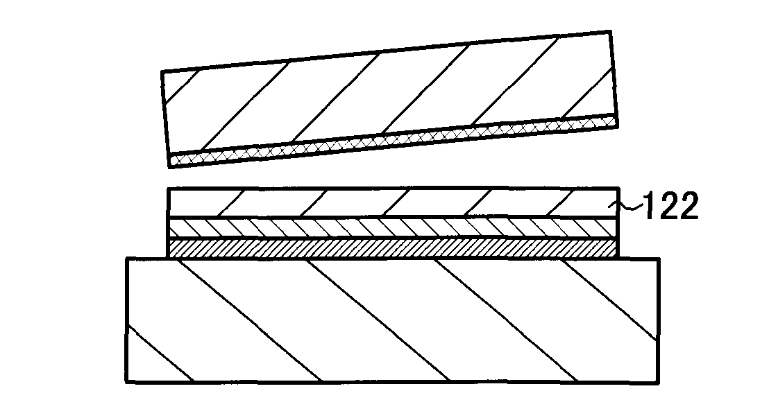
[0110]As an SOI substrate, the SOI substrate manufactured by the method of Embodiment Mode 1 is used here. FIG. 5A is a cross-sectional view of the SOI substrate manufactured by the method described with reference to FIGS. 1A-1 to 1A-4, 1B, 1C, and 1D.

[0111]By element isolation of the single crystal semiconductor layer 122 of the SOI substrate by etching, semiconductor layers 151 and 152 are formed as shown in FIG. 5B. The semiconductor layer 151 is used for forming an n-...


PUM

PropertyMeasurementUnit
temperatureaaaaaaaaaa
surface roughnessaaaaaaaaaa
diameteraaaaaaaaaa

Abstract

An object is to reduce occurrence of defective bonding between a base substrate and a semiconductor substrate even when a silicon nitride film or the like is used as a bonding layer. Another object is to provide a method for manufacturing an SOI substrate by which an increase in the number of steps can be suppressed. A semiconductor substrate and a base substrate are prepared; an oxide film is formed over the semiconductor substrate; the semiconductor substrate is irradiated with accelerated ions through the oxide film to form a separation layer at a predetermined depth from a surface of the semiconductor substrate; a nitrogen-containing layer is formed over the oxide film after the ion irradiation; the semiconductor substrate and the base substrate are disposed opposite to each other to bond a surface of the nitrogen-containing layer and a surface of the base substrate to each other; and the semiconductor substrate is heated to cause separation along the separation layer, thereby forming a single crystal semiconductor layer over the base substrate with the oxide film and the nitrogen-containing layer interposed therebetween.

Description

BACKGROUND OF THE INVENTION[0001]1. Field of the Invention[0002]The present invention relates to a method for manufacturing a silicon-on-insulator (SOI) substrate. The present invention also relates to a semiconductor device manufactured using the SOI substrate.[0003]2. Description of the Related Art[0004]In recent years, integrated circuits using a silicon-on-insulator (SOI) substrate where a thin single crystal semiconductor layer is present over an insulating surface, instead of using a bulk silicon wafer, have been developed. Because parasitic capacitance between a drain of a transistor and a substrate is reduced by use of an SOI substrate, SOI substrates are attracting attention as substrates which improve performance of semiconductor integrated circuits.[0005]One of known methods for manufacturing SOI substrates is a Smart Cut (registered trademark) method (for example, see Reference 1: Japanese Published Patent Application No. 2000-124092). A summary of a method for manufactu...

Claims


Application Information

Patent Timeline
Patent Type & Authority Applications(United States)
IPC IPC(8): H01L21/762
CPCY10S438/977H01L21/76254H01L27/12
Inventor KAKEHATA, TETSUYAKURIKI, KAZUTAKA
Owner SEMICON ENERGY LAB CO LTD
Why Eureka
Try Eureka