
Compositions and method for removing coatings and preparation of surfaces for use in metal finishing, and manufacturing of electronic and microelectronic devices

a technology for metal finishing and coatings, applied in detergent compounding agents, inorganic non-surface active detergent compositions, instruments, etc., can solve the problems of metal-containing residues oxidized and made more difficult to remove, contamination of semiconductor substrate surfaces, etc., and achieve the effect of improving performan

Inactive Publication Date: 2009-05-14
SURFACE CHEM DISCOVERIES
View PDF10 Cites 111 Cited by
  • Summary
  • Abstract
  • Description
  • Claims
  • Application Information

AI Technical Summary

Benefits of technology

The present invention provides a liquid cleaning composition and a method for removing particles, organic contamination, photoresist, post-ash residue, coatings, and other materials from metal and silicon surfaces. The composition contains a strong base, a water soluble organic amine, a water soluble oxidizing agent, and water, and may also contain corrosion inhibitors, surfactants, and chelating agents to enhance performance. The composition has high water content, low cost, and negligible environmental impact. The method involves contacting the surface with the cleaning composition and optionally heating or applying sonic energy. The composition is effective in removing coatings, photopolymers, and photoresists, as well as residues and particles from microelectronic substrates and nano-structures. The composition is also compatible with a variety of metal cleaning applications and reduces solder etch rates and silicon wafer etch rates.

Problems solved by technology

During an ashing process, any metal-containing residues are oxidized and made more difficult to remove.
Unfortunately, chemical mechanical polishing processes leave contamination on the surfaces of the semiconductor substrate, which, like photoresist, must be removed before further elaboration of the integrated circuit.

Method used


Image

  • Compositions and method for removing coatings and preparation of surfaces for use in metal finishing, and manufacturing of electronic and microelectronic devices
  • Compositions and method for removing coatings and preparation of surfaces for use in metal finishing, and manufacturing of electronic and microelectronic devices
  • Compositions and method for removing coatings and preparation of surfaces for use in metal finishing, and manufacturing of electronic and microelectronic devices

Examples


example 20

Removal of Thick Photopolymer from Solder Bumps

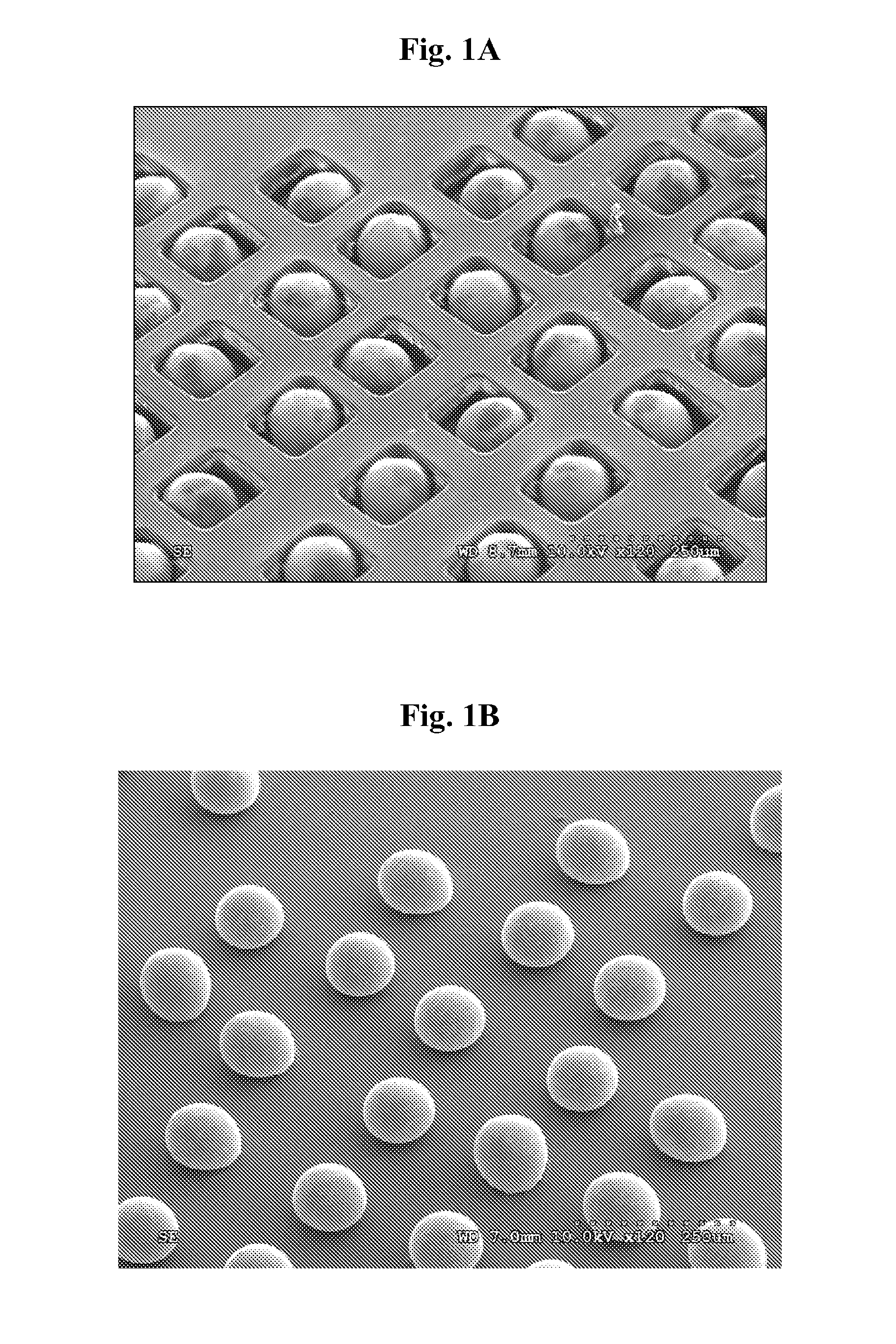
[0068]A 75 μm thick film of Shipley GA-30 dry film photopolymer was laminated to a silicon wafer and patterned. A tin-lead eutectic solder was deposited into the opened features and subsequently heated to reflow. This heating step hardened the photopolymer rendering it difficult to remove using typical solvent mixtures. FIG. 1A is a SEM micrograph of the resulting solder bumps before cleaning. FIG. 1B is a SEM micrograph of the solder bumps after cleaning with the composition according to Example 1a at 65° C. for 30 minutes to remove the photopolymer, followed by a water rinse. The photopolymer was completely removed without affecting the solder bumps. Cleaning with the composition according to Example 1b at 65° C. for 10 minutes followed by a water rinse removed the photopolymer but also removed the solder bumps. Thus without the hydrogen peroxide component, the composition was too aggressive, removing the desired solder bumps as well ...

example 21

Removal of Implanted Photoresist

[0070]Photoresist was applied to a silicon wafer and patterned in the usual way. The patterned wafer was implanted at about 30 KeV with 10e13 of B+ and As+ ions resulting in a very difficult to remove hardened photoresist. Treatment of pieces of this wafer with either the composition according to Example 2 or the composition according to Example 1b at 65° C. for 10 minutes followed by a water rinse completely removed the hardened photoresist. However the composition according to Example 1b caused considerable etching and roughening of the cleaned silicon surface whereas the composition according to Example 2 resulted in a clean and smooth surface.

[0071]An etch rate for the composition according to Example 2 on a silicon wafer at the cleaning temperature of 65° C. was determined to be 0 Å / minute, for the composition according to Example 1b the rate was 8 Å / minute. Thus the addition of hydrogen peroxide eliminated silicon etching protecting the wafer fr...

example 22

Removal of Thin Photoresist

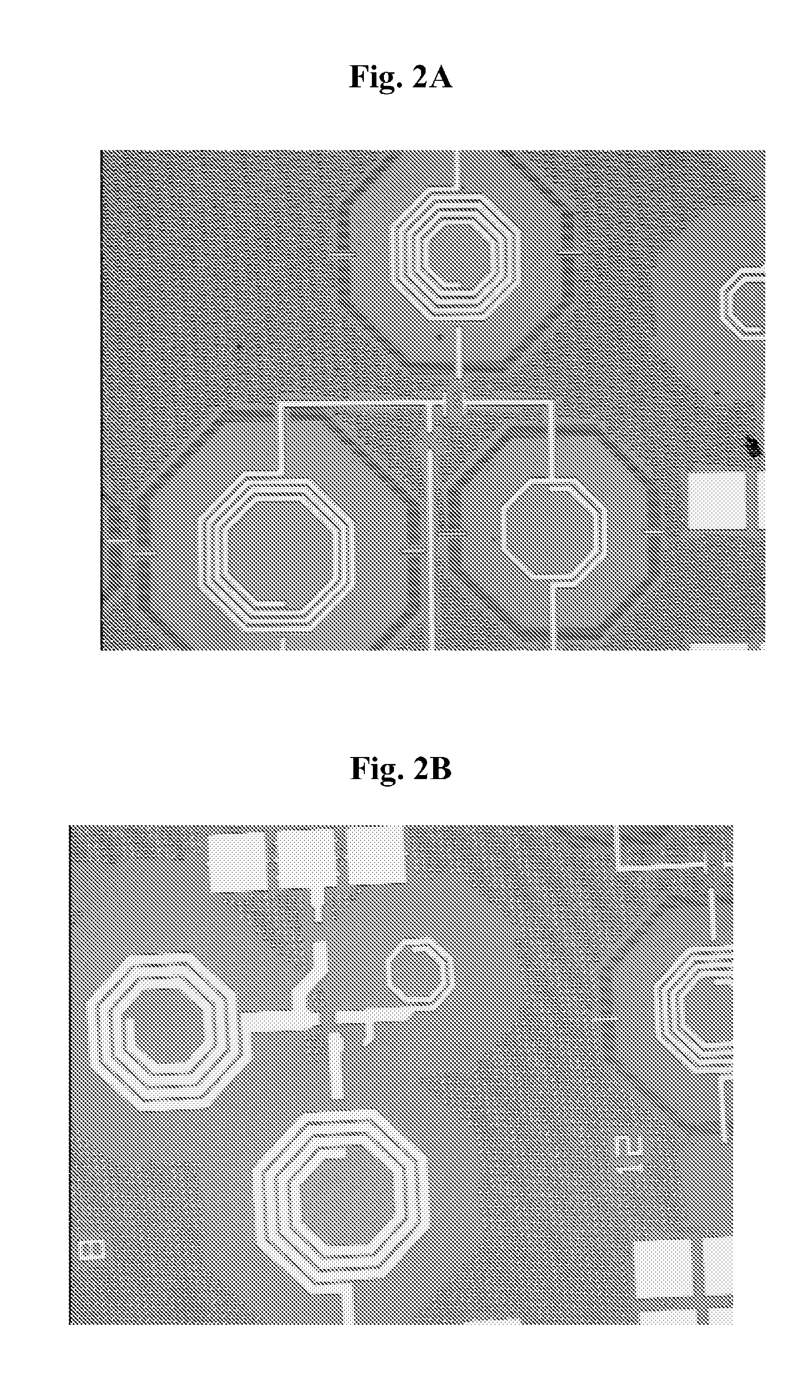
[0072]A silicon wafer was treated to give a 700 nm thick tetraethylorthosilicate (TEOS) film which was topped with 200 nm of SiN then 1650 nm more of TEOS. A 2.4 μm thick film of photoresist was spun onto this surface, baked and patterned. This process hardened the photoresist rendering it impossible to remove using typical solvent mixtures. FIG. 2A is an optical micrograph of the resulting pattern before cleaning. FIG. 2B is an optical micrograph of the pattern after cleaning with a composition according to Example 3 at 75° C. for 10 minutes followed by water rinsing. This treatment completely removed the hardened photoresist. Cleaning with a composition according to Example 1b at 75° C. for 20 minutes had no effect on the photoresist. Thus the presence of an oxidizing agent was necessary to remove the hardened photoresist. The composition according to Example 4, containing 2.4% of hydrogen peroxide, was also effective for removing the photoresist from th...


PUM

PropertyMeasurementUnit
temperatureaaaaaaaaaa
temperaturesaaaaaaaaaa

Abstract

Improved cleaning compositions for removing particles, organic contamination, photoresist, post-ash residue, coatings, and other materials from metal and silicon surfaces including substrates present during the manufacture of integrated circuits, liquid crystal displays, and photovoltaic devices. The cleaning and surface preparation compositions comprise one or more water soluble strongly basic components, one or more water soluble organic amines, one or more water soluble oxidizing agents, balance water. Optional components can include corrosion inhibitors, surfactants and chelating agents.

Description

CROSS REFERENCE TO RELATED APPLICATION(S)[0001]This application claims priority from U.S. Patent Application No. 61 / 002,598 filed Nov. 9, 2007, which is incorporated by reference as if fully set forth.FIELD OF INVENTION[0002]The present invention pertains to removing particles, organic contamination, photoresist, post-ash residue, coatings, and other materials from metal and silicon surfaces including substrates present during the manufacture of integrated circuits, liquid crystal displays, and photovoltaic devices.BACKGROUND OF THE INVENTION[0003]The fabrication of integrated circuits (IC) and other electronic devices such as photovoltaic cells incorporates scores of cleaning sequences involving a large number of toxic, flammable, explosive, and environmentally hazardous chemicals. These include hydrogen fluoride, hydroxylamine, phenols, strong acids, and a broad range of organic solvents. Many of these cleaning agents are also widely used for metal surfaces in variety of applicati...

Claims


Application Information

Patent Timeline
Patent Type & Authority Applications(United States)
IPC IPC(8): C23G1/14G03F7/42
CPCC11D3/3947C11D7/06C11D7/3209G03F7/425C23G1/14C23G1/20C11D11/0047C11D2111/22
Inventor NAGHSHINEH, SHAHRIARYANDERS, KEVINOLDAK, EWASCHWARTZKOPF, GEORGE
Owner SURFACE CHEM DISCOVERIES
Learn More