

Negative resistance field effect element and high-frequency oscillation element
a field effect and negative resistance technology, applied in the direction of oscillator generators, semiconductor devices, electrical apparatus, etc., can solve the problems of limiting control from outside, unsuitable for application to logical devices or as integrated devices, amplifying functions or the like cannot be naturally expected, etc., to achieve negative resistance, large current value, and negative resistance
- Summary
- Abstract
- Description
- Claims
- Application Information
AI Technical Summary
Benefits of technology
Problems solved by technology
Method used
Image

Examples
Embodiment Construction
1. Structure of Negative Resistance Field Effect Device
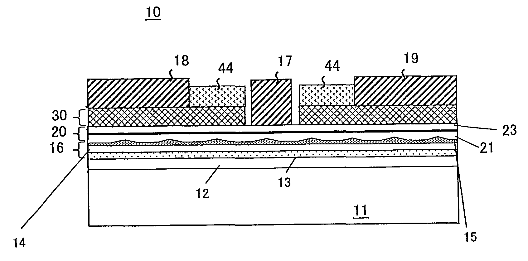
[0028]FIG. 1 is a schematic structural view of an embodiment of a dual-channel negative resistance field effect device. FIG. 1(A) shows the outline of a sectional structure of the dual-channel negative resistance field effect device 10, and FIG. 1(B) shows a detailed sectional layer structure.
[0029]The dual-channel negative resistance field effect device 10 includes an InP substrate 11, an InAlAs buffer layer 12, a double-channel layer 16, a gate Schottky layer 20, a contact layer 30, a gate electrode 17, a source electrode 18, a drain electrode 19, and an SiO2 oxide film 44. Incidentally, the materials of the respective layers are merely examples, and suitable materials can be used. For example, as the substrate, instead of the InP substrate 11, a lattice-matched GaAs substrate may be used, and as the buffer layer 12, AlGaAs may be used. In that case, a GaAs layer may be used as a high-mobility layer 13 of the double-channel la...
PUM
 Abstract
Description
Claims
Application Information