Memory element and memory device

Active Publication Date: 2009-07-09
SONY SEMICON SOLUTIONS CORP
View PDF26 Cites 82 Cited by
  • Summary
  • Abstract
  • Description
  • Claims
  • Application Information

AI Technical Summary

Benefits of technology

[0012]In the memory element or memory device of an embodiment of the present invention, a voltage pulse or a current pulse is applied in the “positive direction” (for example, the first electrode is negative potential and the second electrode is positive potential) to an element in a high resistance state at the time of writing, thereby a conduction path including a metallic element is formed on the first electrode side of the memory layer and the memory layer comes into a low resist

Problems solved by technology

However, the above-mentioned memory element of such a configuration has a disadvantage as follows.
That is, when the element is left for a long time or in a temperature atmosphere higher than room temperature in a storing state where the resistance of the ionic conductor is low (for exa

Method used


Image

  • Memory element and memory device
  • Memory element and memory device
  • Memory element and memory device

Examples


example

Experiment 1

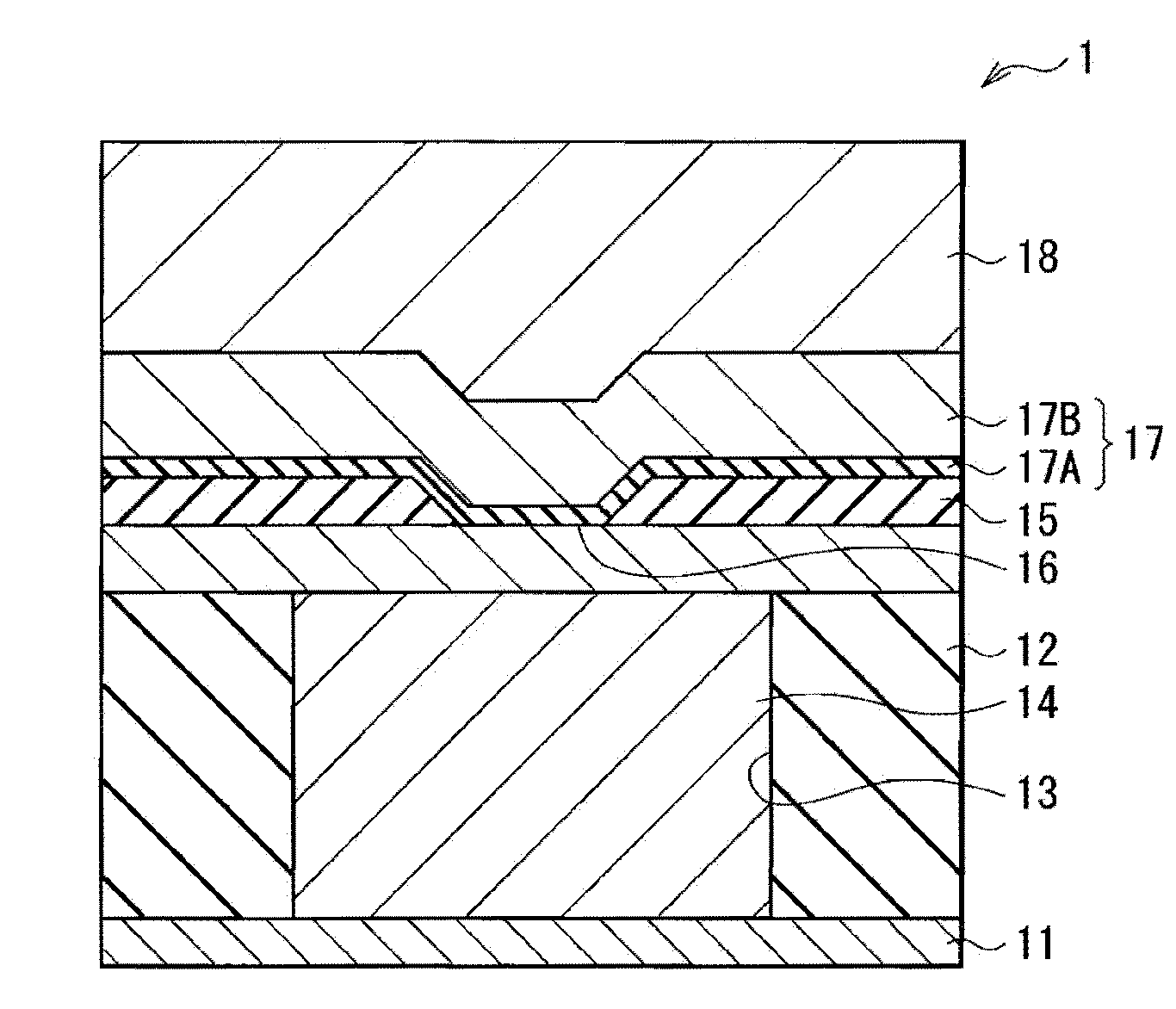
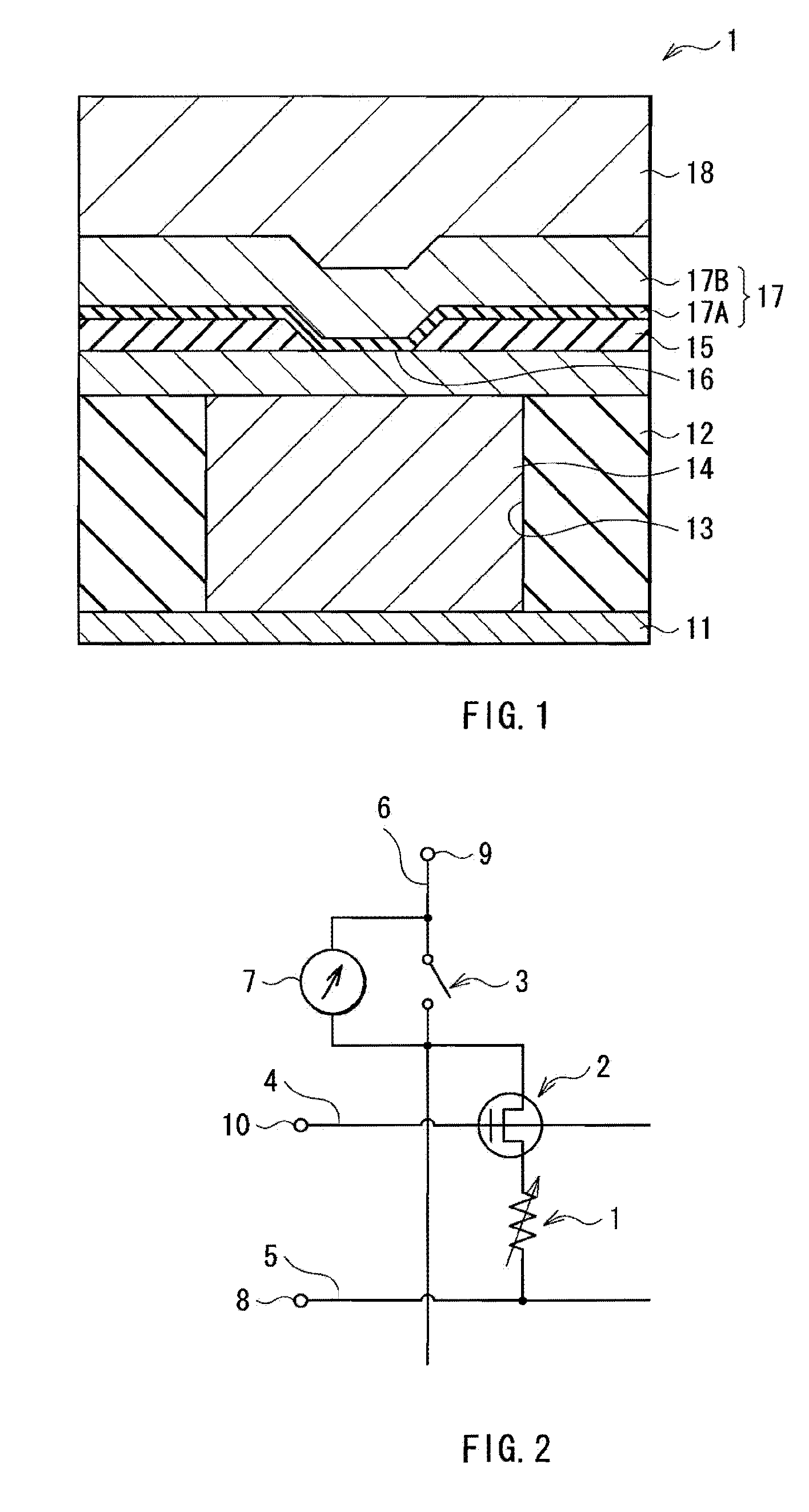
[0049]In order to investigate the effect of introducing oxygen into the above-mentioned ion source layer 17B, a memory element having a sectional structure of FIG. 1 was produced. The lower electrode 14 was made of W, the interlayer insulation film 15 was made of Si3N4, respectively, and the opening 16 of the interlayer insulation film 15 was formed into a round shape of 60 nm in diameter. A GdOx (gadolinium oxide) film was formed to the thickness of 2 nm as the high resistance layer 17B on the interlayer insulation film 15, using a sputtering system, then a Zr16Te44Al40Ox film was formed to the thickness of 45 nm as the ion source layer 17B using Zr, Te and Al (molar ratio: 16:44:40). At this time, a plurality of films were formed simultaneously by variously changing the argon-oxygen concentration. Subsequently, after forming a Zr film and a W film to the thickness of 20 nm as the upper electrode 18 on the ion source layer 17B, patterning was carried out.

[0050]Switching...

experiment 2

[0053]Next, in order to study a possibility of multiple-value recording for the above-mentioned memory element 1, repetitive characteristic for four values was examined on one memory element. Although the layered configuration of the element at that time was the same as the Experiment 1, the round dimension of the opening 16 in the interlayer insulation film 15 of the element was set to 30 nm in diameter. Sputtering conditions were set to the same as the above-mentioned Example 1. The four conductance values were set to 10 μS, 100 μS, 150 μS, and 200 μS, respectively. Recording for higher three conductance levels (100, 150 and 200 μS) was made by writing operation and recording for one lower conductance level (10 μS) was made by erasing operation.

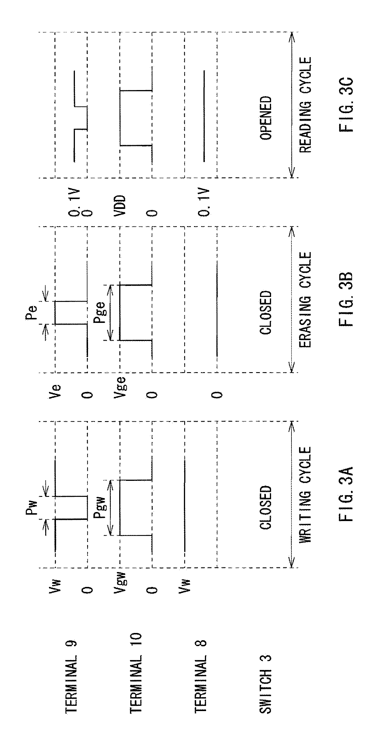
[0054]FIG. 8 illustrates the repetitive characteristics for the four conductance values. Repetition was made by sweeping every pulse 10 sec, both in writing and erasing. The write voltage was set to 2.7 V. The gate voltage was increased eac...

experiment 3

[0055]In order to investigate an appropriate value of oxygen concentration to be introduced into the ion source layer 17B, the following films were formed by Ar sputtering on an oxide film silicon substrate so that elements of different oxygen concentration were produced. The Ar partial pressure at the time of forming Zr16Te44Al40Ox film was set to 0.25 Pa, and oxygen partial pressure was set to 0 Pa (no O2) for Comparative example 2 and 1×10⁻³ Pa (a little O2) for Example 3, and 9.5×10⁻³ Pa (a lot of O2) for Example 4 so that three kinds of samples were produced.

[0056]W film (film thickness: 30 nm) / GdOx film (film thickness: 1.2 nm) / Zr16Te44Al40Ox film (film thickness: 45 nm) / W film (antioxidant film) (film thickness: 5 nm)

[0057]Oxygen concentration in the depth direction was measured about those three kinds of test samples (Comparative example 2 and Examples 3 and 4) using XPS (X-ray photoelectron spectroscopy). The test samples were sputter-etched and their surfaces were analyzed...


PUM


Abstract

A memory device of a resistance variation type, in which data retaining characteristic at the time of writing is improved, is provided. The memory device includes: a plurality of memory elements in which a memory layer is provided between a first electrode and a second electrode so that data is written or erased in accordance with a variation in electrical characteristics of the memory layer; and pulse applying means applying a voltage pulse or a current pulse selectively to the plurality of memory elements. The memory layer includes an ion source layer including an ionic-conduction material and at least one kind of metallic element, and the ion source layer further contains oxygen.

Description

CROSS REFERENCE TO RELATED APPLICATIONS[0001]The present invention contains subject matter related to Japanese Patent Application JP2008-002216 filed in the Japanese Patent Office on Jan. 9, 2008, the entire contents of which being incorporated herein by reference.BACKGROUND OF THE INVENTION[0002]1. Field of the Invention[0003]The present invention relates to a memory element and a memory device with which information (data) is written or erased in accordance with a change in the electrical property of a memory layer including an ion source layer.[0004]2. Description of the Related Art[0005]Examples of a well-known memory device used in information technology device such as a computer include not only a DRAM (Dynamic Random Access memory), which is a memory with high-speed and high-density operation but also non-volatile memory such as a flash memory, FeRAM (Ferroelectric Random Access Memory), and MRAM (Magnetoresistive Random Access Memory). Such memories makes it possible to reta...

Claims


Application Information

Patent Timeline
IPC IPC(8): H01L45/00
CPCG11C13/02G11C2213/11G11C2213/56G11C2213/79H01L27/2436H01L45/1233H01L45/1266H01L45/146H01L45/1625H01L45/085H10B63/30H10N70/245H10N70/8416H10N70/826H10N70/8833H10N70/026
Inventor YASUDA, SHUICHIROTSUSHIMA, TOMOHITOSASAKI, SATOSHIARATANI, KATSUHISA
Owner SONY SEMICON SOLUTIONS CORP
Why Eureka
Try Eureka