System for and method of microwave annealing semiconductor material

a technology of microwave annealing and semiconductor materials, applied in the field of microwave annealing systems and methods, can solve the problems of difficult development of post-annealing processing equipment able to meet operational requirements, subject to end of range (eor) defects, or unrepaired damage, etc., and achieve the effect of facilitating repair

Active Publication Date: 2009-07-23
DSGI
View PDF4 Cites 53 Cited by
  • Summary
  • Abstract
  • Description
  • Claims
  • Application Information

AI Technical Summary

Benefits of technology

[0009]The present invention allows the thermal budget to stay within a desired range to prevent dopant diffusion, in spite of the longer heating times.
[0014]The present invention, in one embodiment, accommodates multiple wafers, i.e. batch processing. Although such an implementation typically utilizes multiple microwave power sources, batch processing allows for increased wafer throughput and can thereby lower the processing cost per wafer. The present invention is capable of simultaneously processing multiple wafers.

Problems solved by technology

Implants that are greater than approximately ˜5 keV and dosages greater than approximately 4E15 atoms / cm3 form an amorphous layer that is re-grown using the post anneal process and are subject to end of range (EOR) defects, or un-repaired damage.
Unfortunately, the post-implantation anneal becomes more challenging due to the limitations of dopant diffusion, the damage recovery percentage, and the thermal budget for the next generation of semiconductor devices.
The development of post annealing processing equipment able to meet operational requirements has been difficult.
Unfortunately, each of these methods are associated with certain problems and disadvantages.
For example, Rapid Thermal Processing is a high-temperature process, i.e., 800 degrees C. to 1100 degrees C., which can cause degradation to the performance of the semiconductor material, as well as an undesired diffusion of the dopant into the surrounding material.
Similarly, Laser Annealing methods are hampered by process integration issues mainly due to the “pattern effects” of the layers.
The volumetric absorption of microwave heating in dielectric lossy materials has been used in a number of different applications, including in the thermal processing of ceramic materials; however, the application to semiconductor materials is rather new and limited.
Heating rates of approximately 100 degrees C. / sec and processing temperatures of approximately 1000 degrees C. over a few seconds were achieved, yet demonstrated no improvement over the RTP techniques.

Method used


Image

  • System for and method of microwave annealing semiconductor material
  • System for and method of microwave annealing semiconductor material
  • System for and method of microwave annealing semiconductor material

Examples


Embodiment Construction

.

BRIEF DESCRIPTION OF THE DRAWING FIGURES

[0018]The present invention is described herein with reference to the following drawing figures, with greater emphasis being placed on clarity rather than scale:

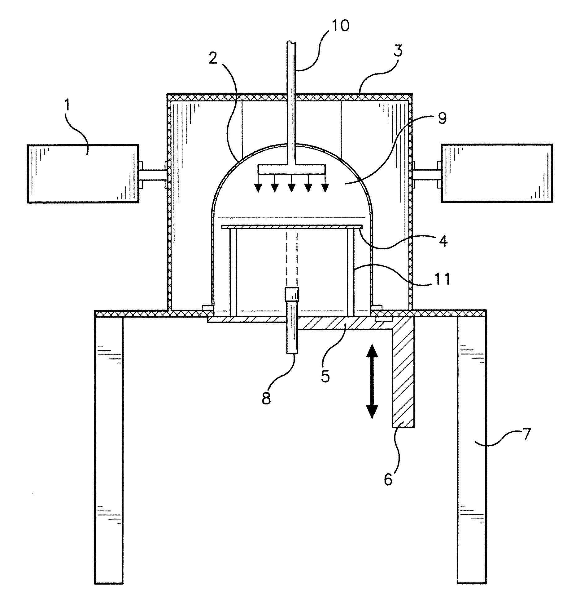
[0019]FIG. 1 is a cross section view of one embodiment of the system;

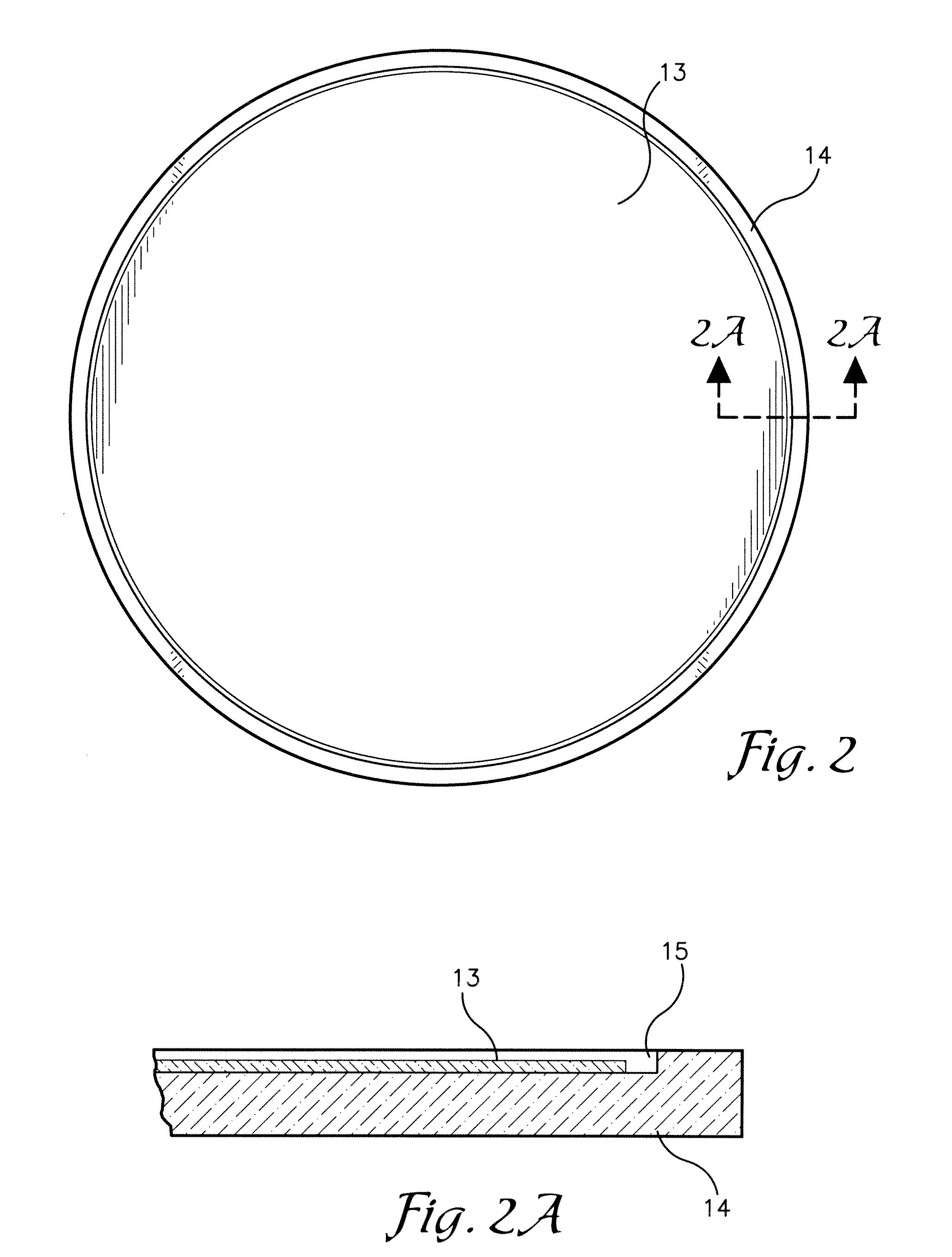
[0020]FIG. 2 is a view of an embodiment of a susceptor plate component of the system;

[0021]FIG. 3 is a Secondary Ion Mass Spectrometry (SIMS) Profile plot of an implant, pre- and post-microwave treatment, showing the effect of no dopant diffusion of the implanted region, along with a comparison of prior art treatment (RTA);

[0022]FIG. 4 is a SIMS profile graph of an Ultra Shallow Junction (USJ) implant, pre- and post-microwave treatment, showing the effect of no dopant diffusion of the implanted region.

[0023]FIG. 5 (a) and (b) are views of Transmission Electron Microscopy (TEM), demonstrating the damage recovery of the present invention treatment, pre- and post-process.

DETAILED DESCRIPTION OF THE INVENTION

[0024]With r...


PUM

PropertyMeasurementUnit
frequencyaaaaaaaaaa
frequencyaaaaaaaaaa
frequencyaaaaaaaaaa

Abstract

A system for and method of processing, i.e., annealing semiconductor materials. By controlling the time, frequency, variance of frequency, microwave power density, wafer boundary conditions, ambient conditions, and temperatures (including ramp rates), it is possible to repair localized damage lattices of the crystalline structure of a semiconductor material that may occur during the ion implantation of impurities into the material, electrically activate the implanted dopant, and substantially minimize further diffusion of the dopant into the silicon. The wafer boundary conditions may be controlled by utilizing susceptor plates (4) or a water chill plate (12). Ambient conditions may be controlled by gas injection (10) within the microwave chamber (3).

Description

RELATED APPLICATIONS[0001]The present non-provisional patent application is related to and claims priority benefit of an earlier-filed non-provisional patent application having the title, THERMAL PROCESSING SYSTEM, COMPONENTS, AND METHODS, application Ser. No. 11 / 559,315, filed Nov. 13, 2006 and an earlier-filed provisional patent application having the title, SYSTEM FOR AND METHOD OF MICROWAVE ANNEALING SEMICONDUCTOR MATERIAL, Ser. No. 60 / 972,898, filed Sep. 17, 2007. The identified earlier-filed applications are hereby fully incorporated by reference into the present application.FIELD OF THE INVENTION[0002]The present invention relates broadly to systems for and methods of processing, i.e., annealing, semiconductor materials. More specifically, the present invention concerns a system for and method of using microwave radiation to activate dopants and to repair damage to the crystalline structure of a semiconductor material that may occur during the ion-implantation of impurities i...

Claims


Application Information

Patent Timeline
Patent Type & Authority Applications(United States)
IPC IPC(8): H01L29/00H01L21/42F27D11/00H05B6/64
CPCH01L21/324H01L21/2636H01L21/67115H01L21/67098
Inventor KOWALSKI, JEFFREY MICHAELKOWALSKI, JEFFREY EDWARD
Owner DSGI
Why Eureka
Try Eureka