Fabricating low cost solder bumps on integrated circuit wafers

a technology of integrated circuits and solder bumps, which is applied in the direction of electrical equipment, semiconductor devices, semiconductor/solid-state device details, etc., can solve the problems of high cost of vacuum deposition process and equipment, high cost of wafer bumping with thin-film ubm processes, and high cost of plating equipment, facilitation, maintenance and bath chemistry maintenance involved in electroless plating processes, etc., to achieve no repassivation layer cost, the effect of lowering the cost o

Inactive Publication Date: 2009-08-20
ATMEL CORP
View PDF6 Cites 14 Cited by
  • Summary
  • Abstract
  • Description
  • Claims
  • Application Information

AI Technical Summary

Benefits of technology

[0011]The simplicity of the disclosed processes provide many advantages, including a lowering of overall product cost when compared with conventional deposited and electroless plated UBM processes. Some examples of cost savings include but are not limited to: a) lower equipment costs and facilitation costs when compared to vacuum deposition equipments, wet-etch lines and plating lines; b) no plating or etching chemical analysis and disposal costs; c) no UBM mask design and mask fabrications costs; d) no repassivation layer costs to “re-shape” the passivation opening; e) no “etch-text” costs as necessary in the electroless UBM process; f) no “full-cassette” charges as necessary in the electroless UBM process; and g) no wafer backside protection layer costs as necessary in the electroless UBM

Problems solved by technology

Vacuum deposition processes and equipment are expensive to purchase, facilitate and maintain.
Moreover, wafer bumping with thin-film UBM processes can be costly.
Similarly, the plating equipment, facilitation, maintenance and bath chemistry maintenance involved in electroless plating processes can be costly.
Additionally, electroless plating processes are often sensitive to variations in the metal bond pad metallurgy (e.g., aluminum) which can cause plating depo

Method used


Image

  • Fabricating low cost solder bumps on integrated circuit wafers
  • Fabricating low cost solder bumps on integrated circuit wafers
  • Fabricating low cost solder bumps on integrated circuit wafers

Examples


example ic

Package Using Solder Bumps with Stud Stumps

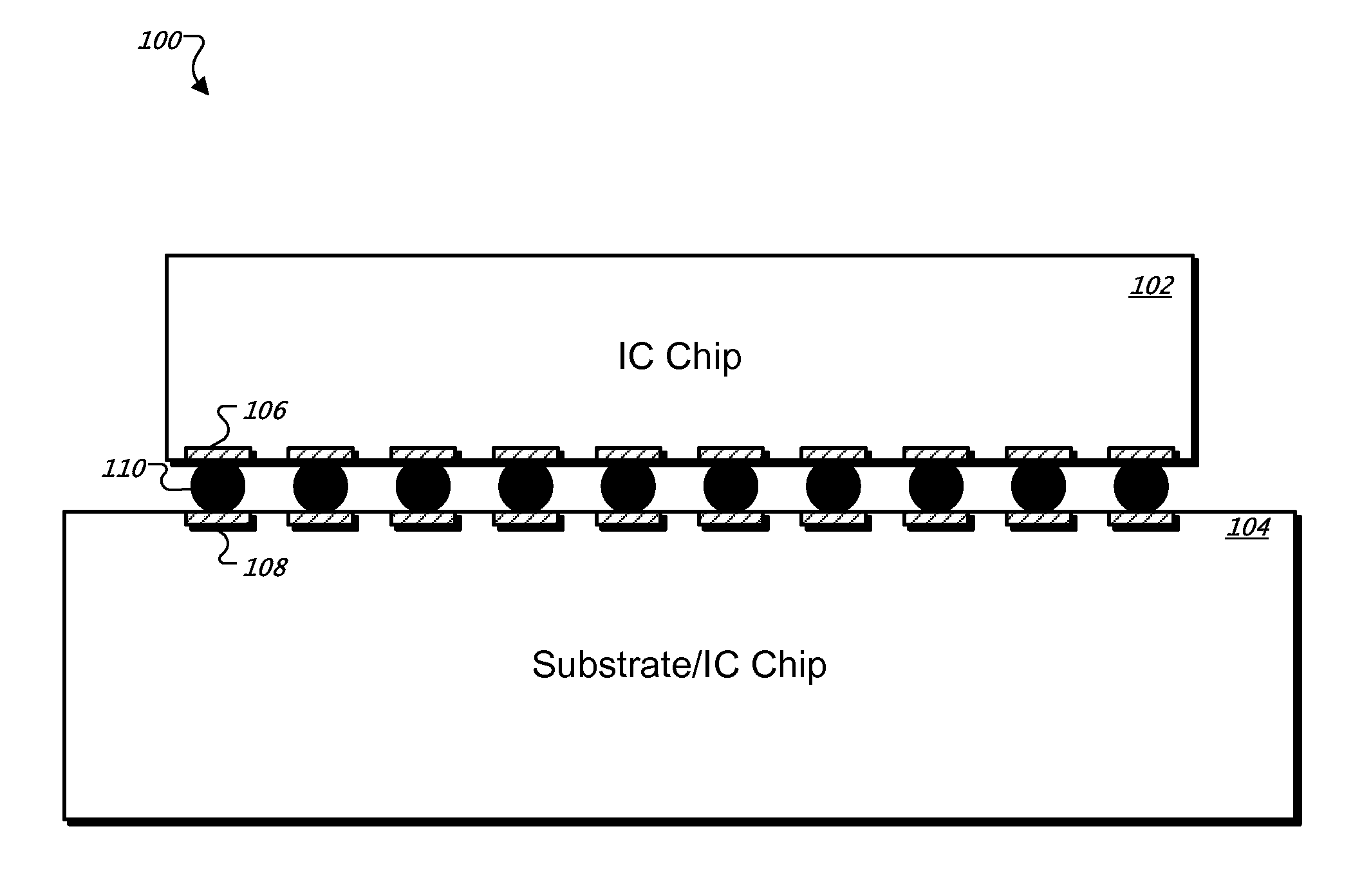
[0019]FIG. 1 illustrates an example IC package 100 including IC chip 102 bonded to substrate 104 using solder bumps 110 which can be fabricated in accordance with processes described in reference to FIGS. 2-4. IC package 100 can be formed using a flip-chip method of interconnection where solder bumps 110 electrically interconnect IC chip 102 to substrate 104 or sometimes to another IC chip.

[0020]Solder bumps 110 are small spheres of solder (solder balls) that can be bonded to contact areas or metal (e.g., aluminum) bond pads 106 formed on a face (circuit side) of IC chip 102 during wafer fabrication, and subsequently face-down bonded with substrate 104. The length of electrical connections between IC chip 102 and substrate 104 can be minimized by: (a) forming solder bumps 110 on bond pads 106; (b) flipping IC chip 102 face-down; (c) aligning solder bumps 110 with bond pads 108 on substrate 104; and (d) reflowing solder balls 110 in a furnac...


PUM


Abstract

A low cost method of forming solder bumps on an integrated circuit (IC) wafer includes depositing solder directly onto stud bumps formed on bond pads of the IC wafer. In some implementations, stud bumps are formed on the IC wafer by performing wire ball-bonding onto metal bond pads of the wafer. Photodefinable solder mask material is applied to the wafer and cured. The photodefinable solder mask material is exposed to form open solder mask areas at the metal bond pad areas. Solder paste is applied into the open solder mask areas. Reflowing the solder paste on the wafer forms solder bumps that wet to the stud bumps. The solder mask is then stripped from the wafer. Other processes (e.g., a wave-soldering machine, stencil or screen printing process) can also be used to wet solder onto stud bumps to form solder bumps.

Description

TECHNICAL FIELD[0001]This subject matter is generally related integrated circuit (IC) wafer processing.BACKGROUND[0002]Wafer-level packaging techniques can include packaging, testing, and performing burn-in operations prior to singulation of the wafer into individual IC chips. During singulation, a dicing machine saws the wafer along scribe lines to separate the individual IC chips. Once an IC chip has been singulated, the IC chip can be mounted on a printed circuit board (PCB).[0003]A typical IC chip uses metal bond pads rather than wires or pins for mounting. The bond pads can be etched or printed onto the wafer, typically along the edges of the package on the face or circuit side of the IC chip. In some implementations, Input / Output (I / O) pads are electrically connected to the bond pads of the IC chip. A redistribution layer (RDL) includes metal lines that can relocate the signals provided by the bond pads to desired locations within the IC chip. Solder bumps can be attached to t...

Claims


Application Information

Patent Timeline
IPC IPC(8): H01L23/52H01L21/44
CPCH01L24/11H01L2924/014H01L2224/16H01L2924/01013H01L2924/01015H01L2924/01029H01L2924/01033H01L2924/01075H01L2924/01078H01L2924/01079H01L2924/01082H01L2924/14H01L2924/30105H01L2924/30107H01L2924/01005H01L2924/01006H01L2224/13099H01L24/05H01L24/06H01L24/13H01L2224/05571H01L2224/05573H01L2224/05624H01L2224/1134H01L2224/13144H01L2924/00014
Inventor LAM, KEN
Owner ATMEL CORP
Why Eureka
Try Eureka