Light-transmitting metal electrode and process for production thereof

Active Publication Date: 2009-08-27
KK TOSHIBA
View PDF25 Cites 25 Cited by
  • Summary
  • Abstract
  • Description
  • Claims
  • Application Information

AI Technical Summary

Benefits of technology

[0100]The openings according to the present invention may be hollow, or otherwise may be filled with substances such as dielectrics. The substances stuffed in the openings are preferably transparent to the incident light.
[0101]The following description is based on the result that a metal electrode having fine openings was produced and measured in practice.
[0102]FIG. 3 is an electron micrograph showing a top surface of the light-transmitting metal electrode comprising openings according to one practical embodiment.
[0103]In this embodiment, silica particles arranged in a monoparticle layer are used to produce a metal electrode. However, if the photo- or electron beam-lithographic processes are improved to produce the similar structure in the future, it can have the same function as the light-transmitting metal electrode according to the present inv

Problems solved by technology

However, since the foil was made of a metal, there was a trade-off relationship between resistivity and light-transmittance and hence it could not have properties satisfying enough to put various devices into practical use.
The problem in metal foil is that the light-transmittance decreases in accordance with increase of the foil thickness, while the problem in oxide semiconductor materials is that the light-transmittance decreases in accordance with increase of the carrier density.
As described above, the demand for light-transmitting metal electrodes is expected to keep expanding in the future in many applications, but there are some future problems.
First, there is a fear that indium, which is employed as a material for the electrodes, will be exhausted.
It is a real f

Method used


Image

  • Light-transmitting metal electrode and process for production thereof
  • Light-transmitting metal electrode and process for production thereof
  • Light-transmitting metal electrode and process for production thereof

Examples


example 1

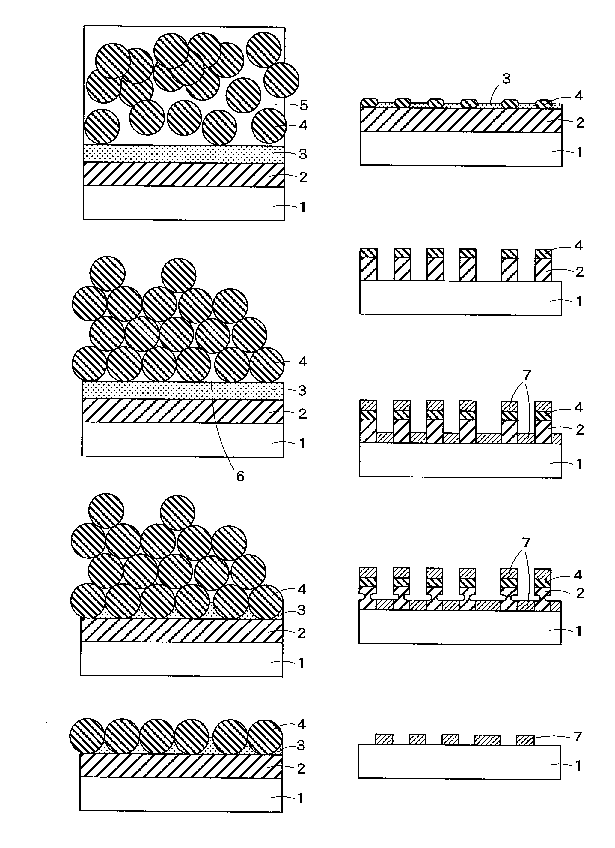
[0121]First, a visible light-transmitting metal electrode was produced.

[0122]The present inventors have found the conditions for preparing a fine silica-monoparticle layer in which plural microdomains having a period of 200 nm are formed. The pattern of the obtained monoparticle layer is transferred to a substrate in the manner described later. Thereafter, a metal electrode is formed by metal vapor-deposition onto the substrate having the transferred pattern, and then the metal deposited in the area of the transferred pattern is removed to produce a light-transmitting metal electrode. Concrete procedures are described below.

[0123]A thermosetting resist (THMR IP3250 [trademark], manufactured by Tokyo Ohka Kogyou Co., Ltd.) was diluted with ethyl lactate by 1:3. The solution was spin-coated at 1500 rpm for 30 seconds on a 4-inch amorphous quartz wafer (Photomask Substrate AQ [trademark], manufactured by Asahi Glass Co., Ltd.), and then heated on a hot-plate at 110° C. for 90 seconds, ...

example 2

[0131]Another visible light-transmitting metal electrode in which the area occupied by Al was reduced was produced. In this electrode, the ratio of the area occupied by the openings was increased to disturb the period and hence to weaken the wavelength dependence of transmitted light.

[0132]First, a thermosetting resist (THMR IP3250 [trademark], manufactured by Tokyo Ohka Kogyou Co., Ltd.) was diluted with ethyl lactate by 1:3. The solution was spin-coated at 1500 rpm for 30 seconds on a 4-inch amorphous quartz wafer (Photomask Substrate AQ [trademark], manufactured by Asahi Glass Co., Ltd.), and then heated on a hot-plate at 110° C. for 90 seconds, and further heated at 250° C. for 1 hour in an oxidation-free inert oven under nitrogen gas-atmosphere to perform a thermosetting reaction. The layer thus formed had a thickness of approx. 120 nm.

[0133]The thermosetting resist (THMR IP3250 [trademark], manufactured by Tokyo Ohka Kogyou Co., Ltd.) was again diluted with ethyl lactate by 1:...

example 3

[0138]This example describes a mass-production method utilizing nano-in-print technology. For the purpose of easy understanding, the method is explained with FIG. 8 referred to. However, in practical applications, minor conditions may be changed from those described below. In this method, the columnar pattern of fine silica particles is used as a mold to produce a Ni-made stamper for nano-in-print.

[0139]First, a thermosetting resist (THMR IP3250 [trademark], manufactured by Tokyo Ohka Kogyou Co., Ltd.) was diluted with ethyl lactate by 1:3. The solution was spin-coated at 1500 rpm for 30 seconds on a 6-inch silicon wafer 11, and then heated on a hot-plate at 110° C. for 90 seconds, and further heated at 250° C. for 1 hour in an oxidation-free inert oven under nitrogen gas-atmosphere to perform a thermosetting reaction. The layer 12 thus formed had a thickness of approx. 120 nm.

[0140]The thermosetting resist (THMR IP3250 [trademark], manufactured by Tokyo Ohka Kogyou Co., Ltd.) was a...


PUM


Abstract

The present invention provides a light-transmitting metal electrode including a substrate and a metal electrode layer having plural openings. The metal electrode layer also has such a continuous metal part that any pair of point-positions in the part is continuously connected without breaks. The openings in the metal electrode layer are periodically arranged to form plural microdomains. The plural microdomains are so placed that the in-plane arranging directions thereof are oriented independently of each other. The thickness of the metal electrode layer is in the range of 10 to 200 nm.

Description

CROSS-REFERENCE TO RELATED APPLICATIONS[0001]This application is based upon and claims the benefit of priority from the prior Japanese Patent Applications No. 42894 / 2008, filed on Feb. 25, 2008; the entire contents of which are incorporated herein by reference.BACKGROUND OF THE INVENTION[0002]1. Field of the Invention[0003]The present invention relates to a light-transmitting metal electrode. In detail, the invention relates to a light-transmitting metal electrode having a hyperfine structure. The present invention also relates to a process for production of the light-transmitting metal electrode.[0004]2. Background Art[0005]Light-transmitting metal electrodes, which have light transparency particularly in the visible region and at the same time which function as electrodes, are widely used in electronics industries. For example, all the displays distributed currently in markets, except displays of cathode ray tube (CRT) type, need light-transmitting metal electrodes since they adop...

Claims


Application Information

Patent Timeline
IPC IPC(8): H01B5/00H01J9/00H01B5/14H01B13/00H01J9/02H01J11/22H01J11/34
CPCH01J1/02H01J9/02H01B13/0036H01J63/02H01J2217/49207H01J17/04
Inventor TSUTSUMI, EISHINAKANISHI, TSUTOMUFUJIMOTO, AKIRAASAKAWA, KOJI
Owner KK TOSHIBA
Why Eureka
Try Eureka