Gallium nitride-based compound semiconductor light-emitting device

a compound semiconductor and light-emitting device technology, applied in the direction of semiconductor devices, basic electric elements, electrical apparatus, etc., can solve the problems of high contact resistance, low operating voltage, high resistance in diffusion direction, etc., to achieve good crystallinity of semiconductors, reduce contact resistance between semiconductors and transparent electrically conducting film layers, and reduce the effect of resistan

Active Publication Date: 2009-09-10
TOYODA GOSEI CO LTD
View PDF9 Cites 12 Cited by
  • Summary
  • Abstract
  • Description
  • Claims
  • Application Information

AI Technical Summary

Benefits of technology

[0031]The gallium nitride-based compound semiconductor light-emitting device of the present invention appropriately has a semiconductor metal mixed layer containing a Group III metal, constituting the semiconductor, on the semiconductor side surface of the transparent electrically conducting film layer constituting the positive electrode, so that the contact resistance between the positive electrode and the p-type semiconductor layer can be small. Also, in the semiconductor metal mixed layer, a large concentration gradient of the semiconductor metal is generated to have a high semiconductor metal proportion in the vicinity of the semiconductor/transparent electrically conducting film layer interface and a low semiconductor metal proportion at the posi

Problems solved by technology

When a metal is formed into a thin film, there arises a problem that the resistance in the diffusion direction becomes high.
In the sputtering method, the contact re

Method used


Image

  • Gallium nitride-based compound semiconductor light-emitting device
  • Gallium nitride-based compound semiconductor light-emitting device
  • Gallium nitride-based compound semiconductor light-emitting device

Examples


example 1

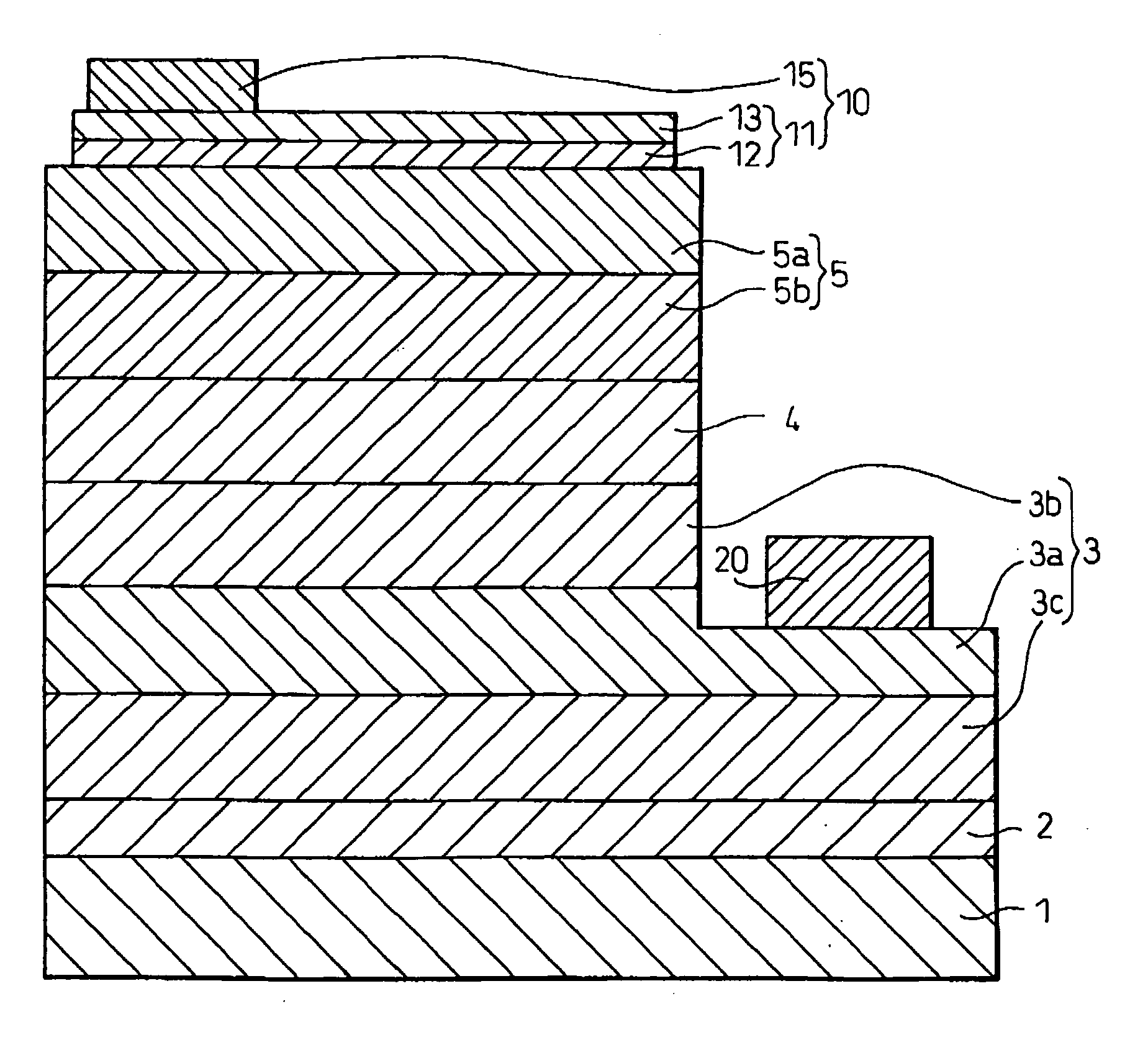
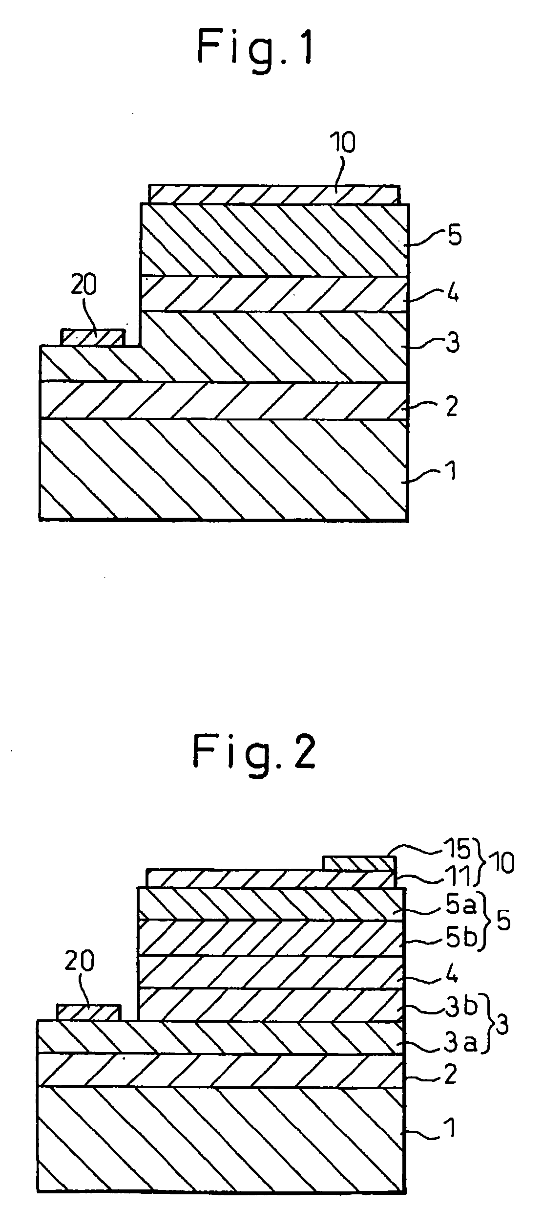
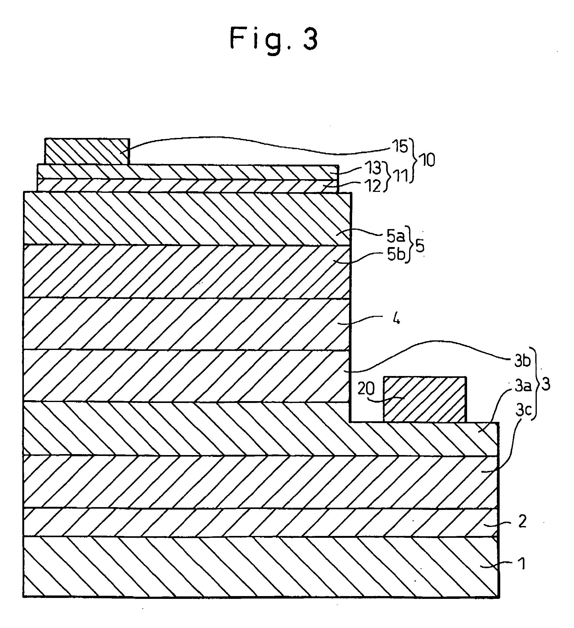
[0079]FIG. 3 is a schematic view showing the cross-section of a gallium nitride-based compound semiconductor light-emitting device produced in this Example, and FIG. 4 is a schematic view showing the planar surface thereof. An n-type semiconductor layer (3) consisting of a 3 μm-thick underlying layer (3c) composed of undoped GaN, a 2 μm-thick n-type contact layer (3a) composed of Si-doped n-type GaN and a 0.03 μm-thick n-type clad layer (3b) composed of n-type In0.1Ga0.9N, a light-emitting layer (4) having a multi-quantum well structure in which a 0.03 μm-thick barrier layer composed of Si-doped GaN and a 2.5 nm-thick well layer composed of In0.2Ga0.8N were stacked five times and the barrier layer was finally provided, and a p-type semiconductor layer (5) consisting of a 0.05 μm-thick p-type clad layer (5b) composed of Mg-doped p-type Al0.07Ga0.93N and a 0.15 μm-thick p-type contact layer (5a) composed of Mg-doped p-type GaN were sequentially stacked on a sapphire substrate (1) thro...

examples 2 and 3

[0091]Gallium nitride-based compound semiconductor light-emitting devices were produced in the same manner as in Example 1 except for changing the film formation condition of the positive electrode (the pressure of the sputtering apparatus at the formation of the transparent electrically conducting film contact layer), and the device characteristics were evaluated. The results obtained are shown in Table 1 together with the results of Example 1. Incidentally, in these light-emitting devices, the thickness of the positive electrode metal mixed layer was from 1 to 5 nm, and the proportion of the positive electrode metal was from 0.5 to 18%. As for the semiconductor metal mixed layer, these are shown in Table 1.

TABLE 1Pressure atFormation ofSemiconductor Metal Mixed LayerTransparentProportion of Semiconductor Metal [at. %]Device CharacteristicsElectricallyPortion of 1 nm fromPortion of 3 nm fromForwardLightconducting FilmThicknessp-Type Contact Layerp-Type Contact LayerVoltageEmissionC...

example 4

[0092]A gallium nitride-based compound semiconductor light-emitting device was produced in the same manner as in Example 1 except for not performing the heat treatment after the formation of the positive electrode. Its device characteristics are shown also in Table 1.


PUM


Abstract

An object of the present invention is to provide a gallium nitride-based compound semiconductor light-emitting device with low driving voltage and high light emission output, which has a positive electrode comprising a transparent electrically conducting layer put into direct contact with a p-type semiconductor layer.
The inventive gallium nitride-based compound semiconductor light-emitting device comprises an n-type semiconductor layer, a light-emitting layer and a p-type semiconductor layer which are formed in this order on a substrate, wherein each layer comprises a gallium nitride-based compound semiconductor, the light-emitting device has a negative electrode and a positive electrode provided on the n-type semiconductor layer and on the p-type semiconductor layer, respectively, the positive electrode is at least partially formed of a transparent electrically conducting film, the transparent electrically conducting film is at least partially in contact with the p-type semiconductor layer, a semiconductor metal mixed layer containing a Group III metal component is present on the semiconductor side surface of the transparent electrically conducting film, and the thickness of the semiconductor metal mixed layer is from 0.1 to 10 nm.

Description

CROSS REFERENCE TO RELATED APPLICATION[0001]This application is an application filed under 35 U.S.C. §111(a) claiming benefit, pursuant to 35 U.S.C. §119(e)(1), of the filing date of the Provisional Application No. 60 / 739,003 filed on Nov. 23, 2005, pursuant to 35 U.S.C. §111(b).TECHNICAL FIELD[0002]The present invention relates to a gallium nitride-based compound semiconductor light-emitting device. More specifically, the present invention relates to a face-up type gallium nitride-based compound semiconductor light-emitting device equipped with a positive electrode having excellent light-transparency and ohmic properties.BACKGROUND ART[0003]In recent years, a GaN-based compound semiconductor material has attracted attention as a semiconductor material for short-wavelength light-emitting devices. The GaN-based compound semiconductor is formed on various oxide substrates such as sapphire single crystal or a Group III-V compound substrate by a metal organic chemical vapor deposition m...

Claims


Application Information

Patent Timeline
IPC IPC(8): H01L33/00H01L33/14H01L33/32H01L33/40H01L33/42
CPCH01L33/32H01L33/42H01L33/40
Inventor KAMEI, KOJI
Owner TOYODA GOSEI CO LTD
Why Eureka
Try Eureka