Plasma processing apparatus and method for manufacturing semiconductor device

a processing apparatus and semiconductor technology, applied in the direction of electrolysis components, vacuum evaporation coatings, coatings, etc., can solve the problems of increasing the defect density of amorphous semiconductor layers, and reducing the mobility of electric fields, so as to achieve high efficiency, high efficiency, and high reliability of electric characteristics.

Active Publication Date: 2009-09-17
SEMICON ENERGY LAB CO LTD
View PDF55 Cites 17 Cited by
  • Summary
  • Abstract
  • Description
  • Claims
  • Application Information

AI Technical Summary

Benefits of technology

[0037]It is possible to provide a plasma processing apparatus by which a semiconductor film having crystallinity even in a film formation step, typically, a microcrystalline semiconductor film is formed and favorable film quality is realized. In addition, a semiconductor...

Problems solved by technology

These elements increase defect density in an amorphous semiconductor layer and decrease electric-field-effect mobility.
In addition, there is a problem in that the surfaces of crystal grains of a microcrystalline semiconductor film that is obtained are easily oxidized.
When cr...

Method used


Image

  • Plasma processing apparatus and method for manufacturing semiconductor device
  • Plasma processing apparatus and method for manufacturing semiconductor device
  • Plasma processing apparatus and method for manufacturing semiconductor device

Examples


embodiment 1

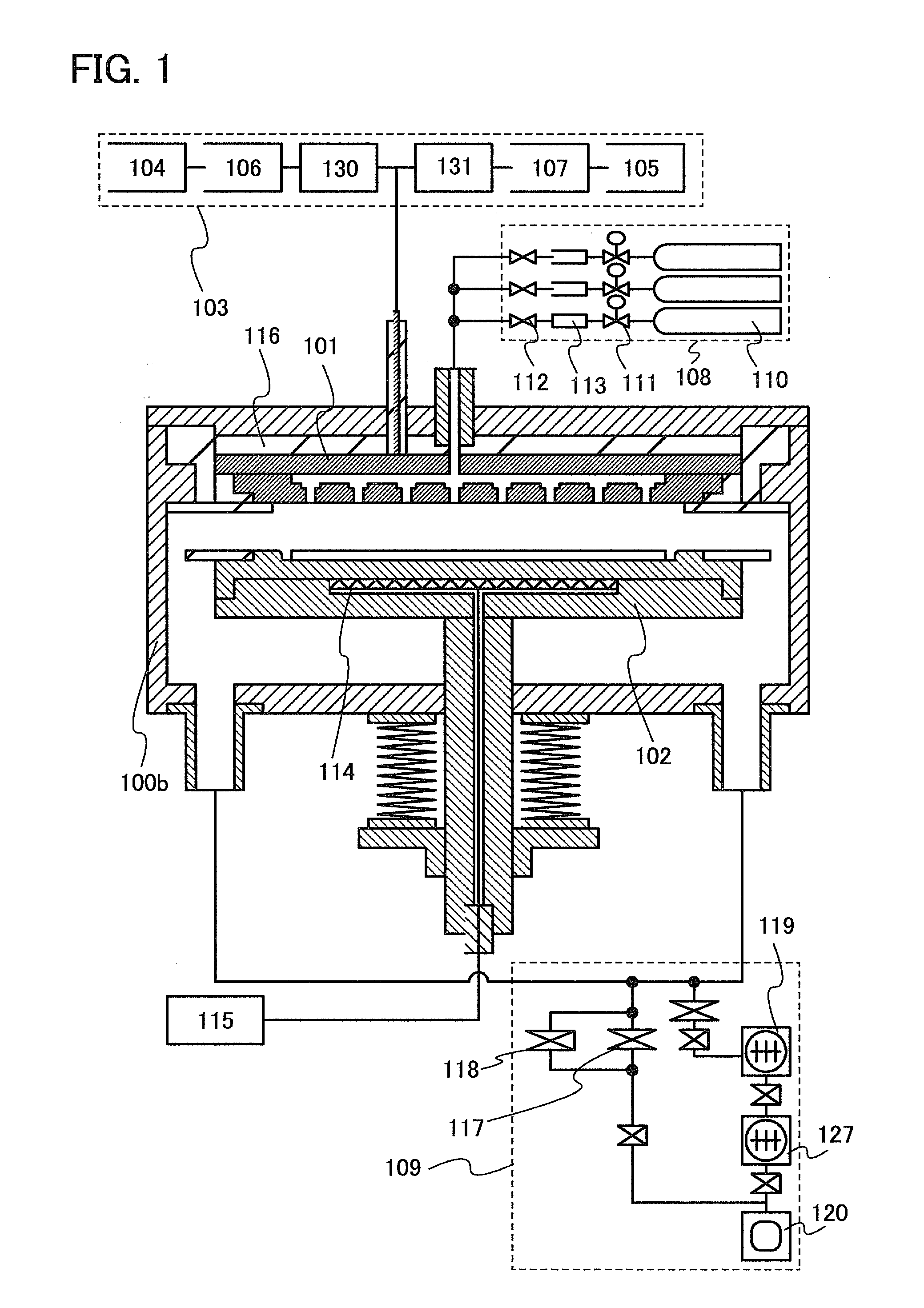
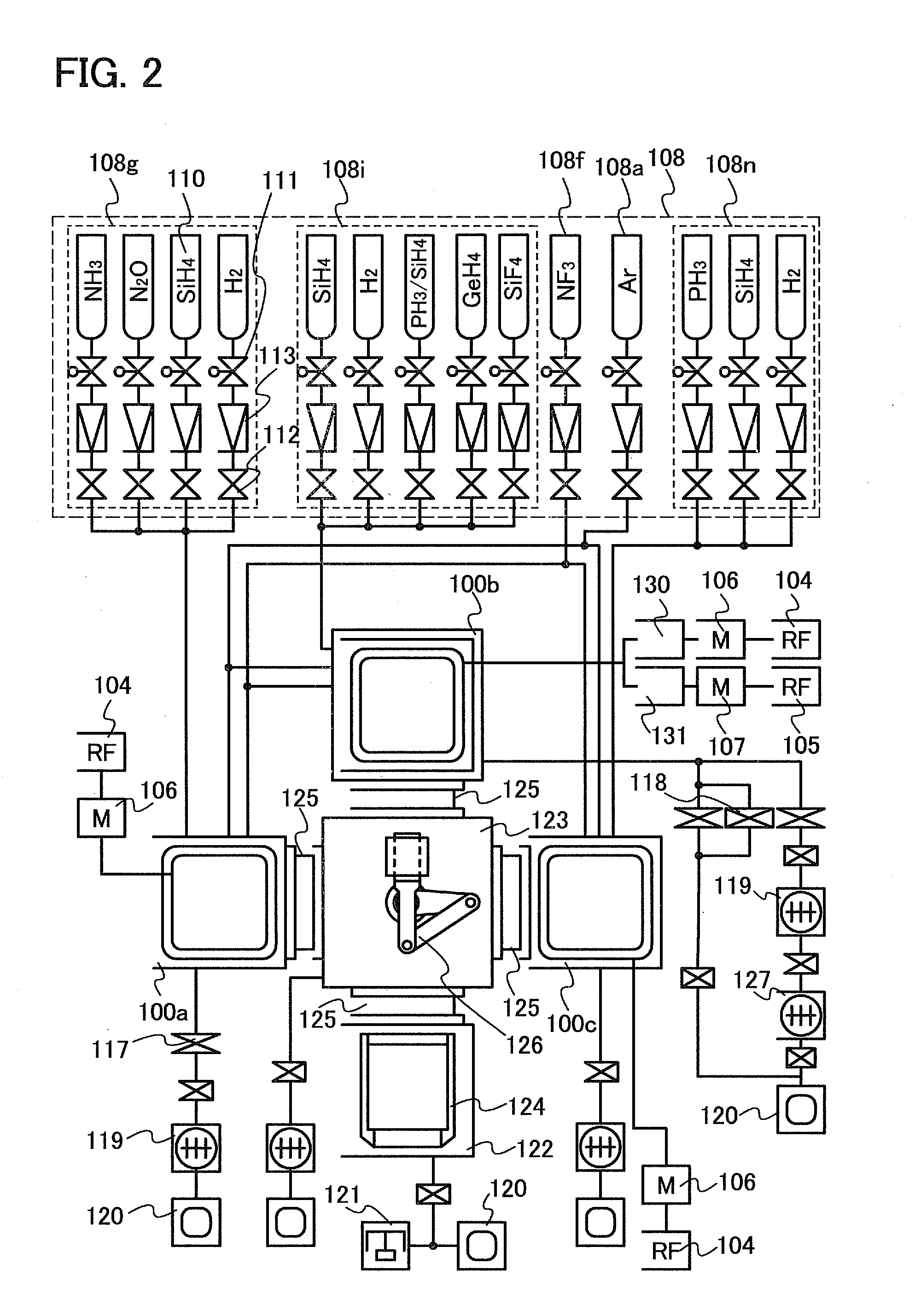
[0058]FIG. 1 illustrates a structural example of a plasma processing apparatus where plural kinds of high-frequency powers are applied. A reaction chamber 100b is formed from a rigid material such as aluminum or stainless steel and can be evacuated to vacuum. In this embodiment, the reaction chamber is formed using stainless steel in order to increase its strength, and the inside thereof is coated with aluminum by thermal spraying. In addition, the reaction chamber can be disassembled for maintenance, and the inside thereof is regularly recoated with aluminum by thermal spraying. The reaction chamber 100b is provided with a first electrode (also referred to as an upper electrode) 101 and a second electrode (also referred to as a lower electrode) 102.

[0059]A high-frequency power supply unit (means) 103 is connected to the first electrode 101, a ground potential is applied to the second electrode 102, and a substrate can be placed on the second electrode 102. The first electrode 101 i...

embodiment 2

[0083]In this embodiment, a manufacturing process of a thin film transistor used for a liquid crystal display device will be described with reference to FIGS. 3A and 3B, FIGS. 4A to 4D, FIGS. 5A to 5C, and FIG. 6. FIGS. 3A and 3B, FIGS. 4A to 4D, and FIGS. 5A to 5C are cross-sectional views illustrating a manufacturing process of a thin film transistor, and FIG. 6 is a top view illustrating a connection region of a thin film transistor and a pixel electrode in one pixel.

[0084]As illustrated in FIG. 3A, a gate electrode obtained by stacking metal layers is formed over a substrate 50.

[0085]As the substrate 50, a plastic substrate having heat resistance that can withstand a process temperature of this manufacturing process or the like can be used, in addition to a non-alkaline glass substrate manufactured by a fusion method or a float method such as a substrate of a barium borosilicate glass, an aluminoborosilicate glass, or an aluminosilicate glass, and a ceramic substrate. In additio...

embodiment 3

[0118]In this embodiment, a manufacturing process of a thin film transistor which has a different structure from that of Embodiment 2 and in which high-speed operation can be performed, an on-state current is large, and an off-state current is small will be described.

[0119]An n-channel thin film transistor having an amorphous semiconductor layer or a microcrystalline semiconductor layer is more suitable for use in a driver circuit than a p-channel one because it has higher field-effect mobility. It is preferable that all thin film transistors formed over the same substrate have the same polarity, in order to reduce the number of manufacturing steps. In this embodiment, description is made using an n-channel thin film transistor.

[0120]A manufacturing process of a thin film transistor will be described with reference to FIGS. 7A to 7E, FIGS. 8A to 8C, FIGS. 9A to 9D, and FIG. 10. Note that the left sides of FIGS. 7A to 7E and FIGS. 8A to 8C are each a cross-sectional view taken along ...


PUM

PropertyMeasurementUnit
Pressureaaaaaaaaaa
Pressureaaaaaaaaaa
Lengthaaaaaaaaaa

Abstract

By an evacuation unit including first and second turbo molecular pumps connected in series, the ultimate pressure in a reaction chamber is reduced to ultra-high vacuum. By a knife-edge-type metal-seal flange, the amount of leakage in the reaction chamber is reduced. A microcrystalline semiconductor film and an amorphous semiconductor film are stacked in the same reaction chamber where the pressure is reduced to ultra-high vacuum. By forming the amorphous semiconductor film covering the surface of the microcrystalline semiconductor film, oxidation of the microcrystalline semiconductor film is prevented.

Description

BACKGROUND OF THE INVENTION[0001]1. Field of the Invention[0002]The present invention relates to a method for manufacturing a semiconductor device which has a circuit including a thin film transistor (hereinafter also referred to as a TFT) using a semiconductor film. In addition, the present invention relates to a plasma processing apparatus for a plasma CVD method used in a process for forming a thin film in manufacturing a semiconductor device. The present invention further relates to a film formation method which uses the plasma processing apparatus. For example, the present invention relates to a photoelectric conversion device typified by a solar cell or a sensor, an electro-optical device typified by a liquid crystal display panel, a light-emitting device including a light-emitting element, or an electronic device equipped with a wireless chip including an antenna as a component.[0003]In this specification, a semiconductor device refers to all types of devices which can functi...

Claims


Application Information

Patent Timeline
IPC IPC(8): H01L21/205C23C14/34
CPCC23C16/24C23C16/509H01L21/67207H01L27/1214H01L27/1288H01L29/78669H01L29/78678H01L29/78696H01L29/04H01L27/127
Inventor FURUNO, MAKOTOSUGIYAMA, TETSUONOZAWA, TAICHIICHIJO, MITSUHIROTAJIMA, RYOTAYAMAZAKI, SHUNPEI
Owner SEMICON ENERGY LAB CO LTD
Why Eureka
Try Eureka