

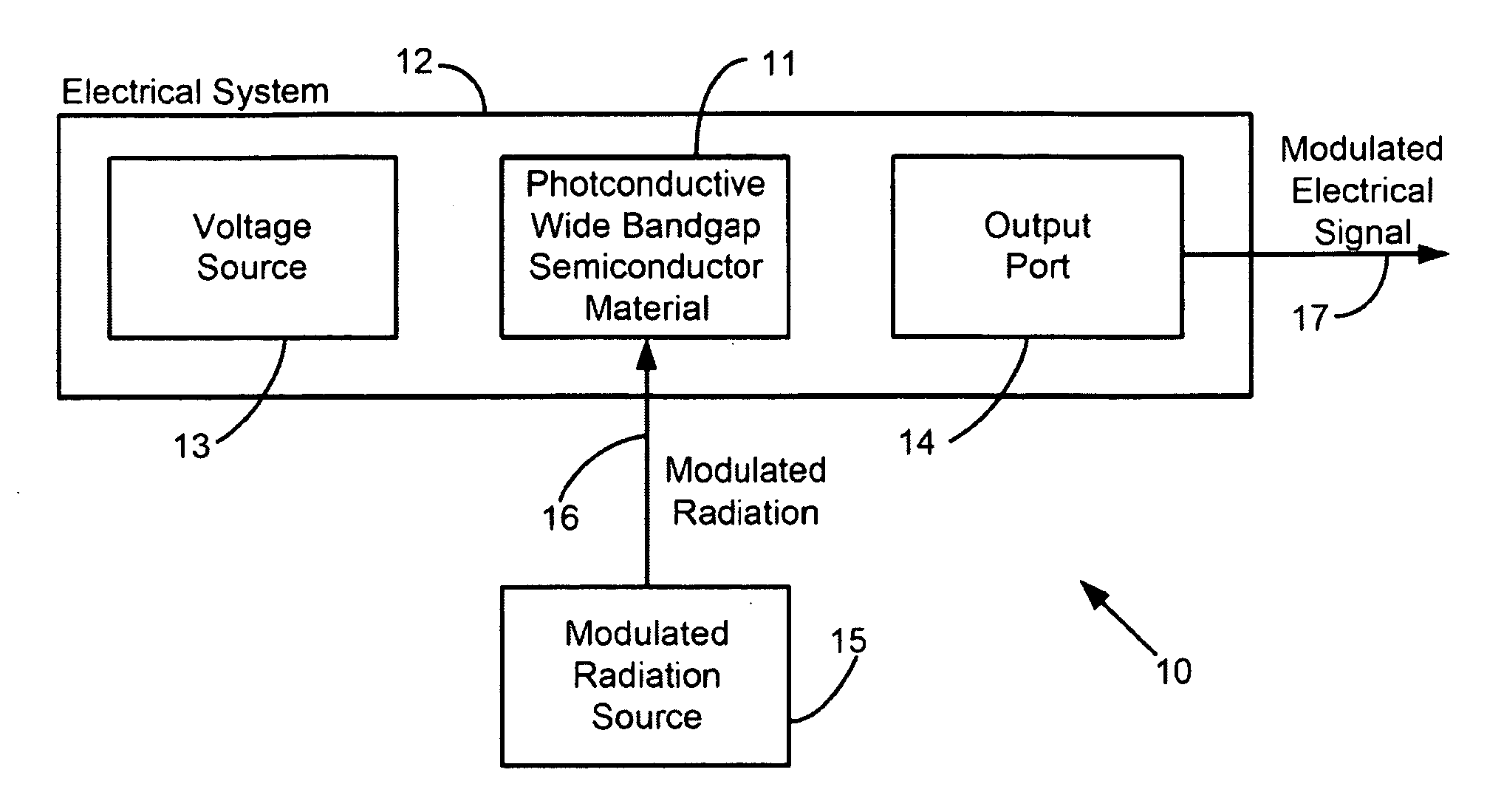
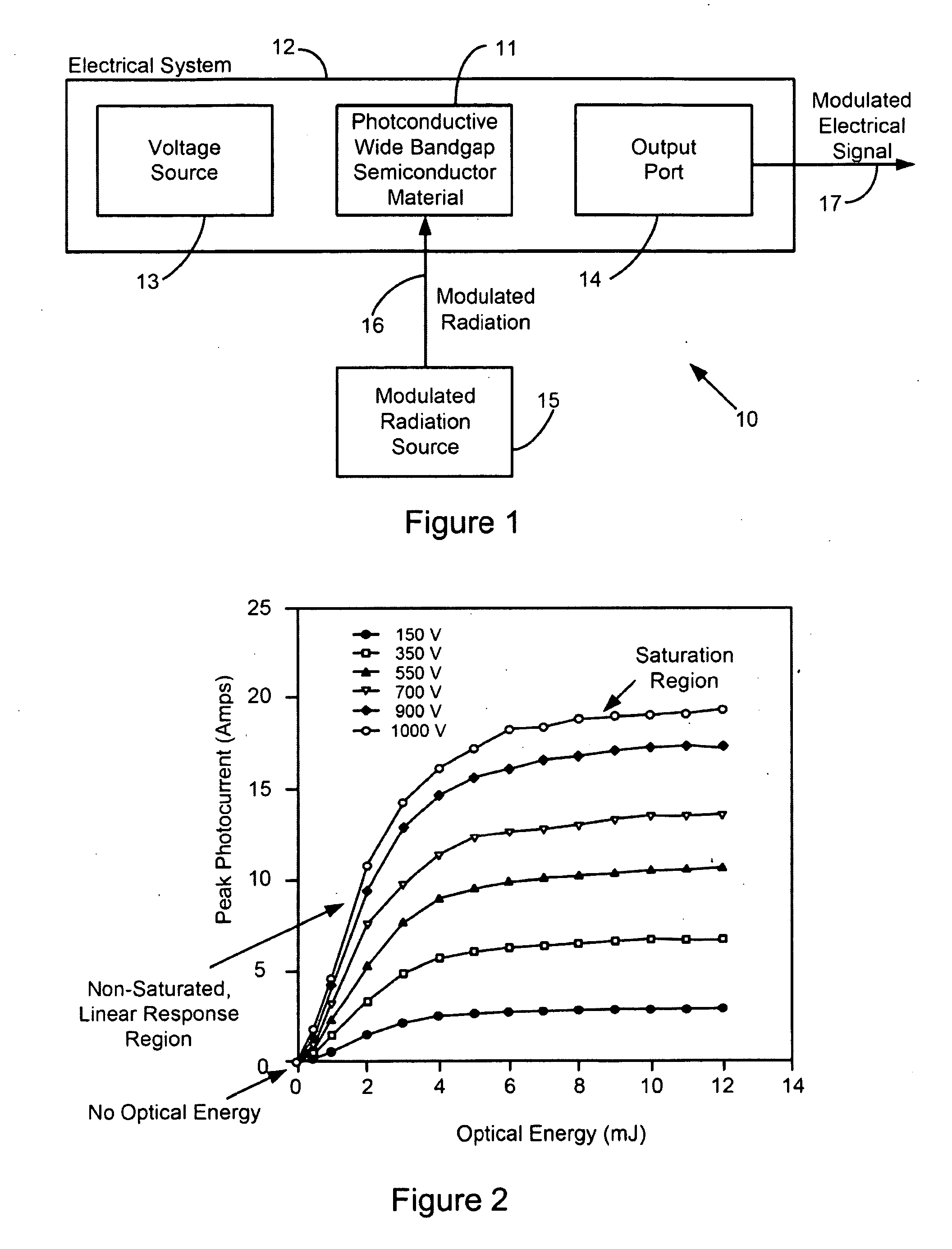
System and method of modulating electrical signals using photoconductive wide bandgap semiconductors as variable resistors
a wide bandgap semiconductor and variable resistor technology, applied in electromagnetic wave modulation, optical radiation measurement, instruments, etc., can solve the problems of low radiated energy, communication fratricide, inconvenient use, etc., and achieve linear response, high current, and high current
- Summary
- Abstract
- Description
- Claims
- Application Information
AI Technical Summary
Benefits of technology
Problems solved by technology
Method used
Image

Examples
example application
ed Particles
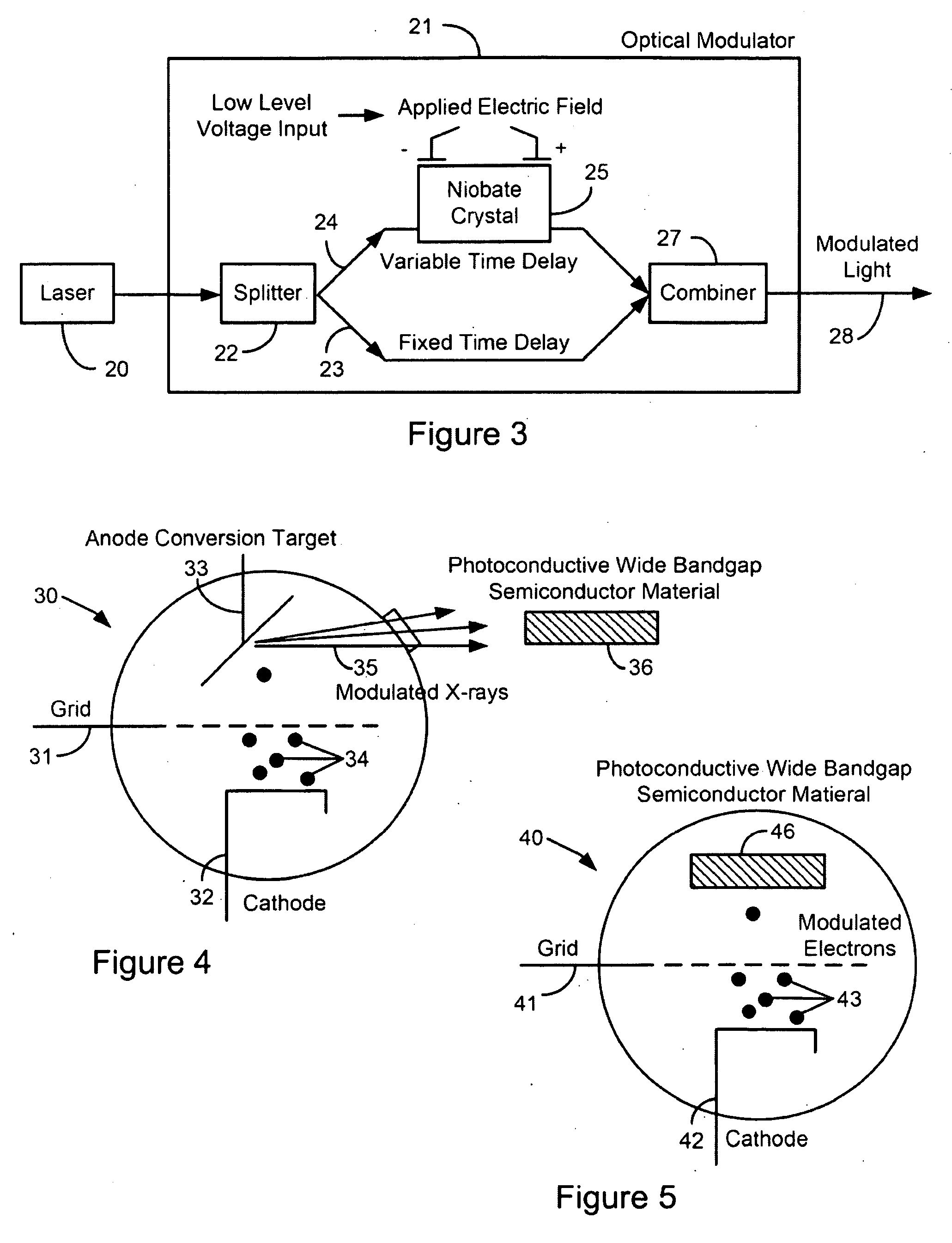
[0052]The modulation of charged particle beams has historically been a critical area of interest. In the case of electron beams, this is especially true, because of the ability of modulated electron beams to produce high-power coherent electromagnetic radiation. Modulation of beams can be divided into density modulation, in which the density of the beam varies along its length, and velocity or energy modulation, in which the energy of a beam (and its velocity, for nonrelativistic beams) varies along its length. A number of techniques have been used to generate modulated beams, such as the use of modulated voltage on grids (as in triodes), or interaction with electromagnetic fields in resonant cavities (such as in klystrons) or slow wave structures (such as in traveling wave tubes). Generally, modulated lasers have not been used to generate modulated particle beams. One exception to this is the use of a modulated laser to produce modulated electron beams through photoemis...
PUM
| Property | Measurement | Unit |
|---|---|---|
| Electric potential / voltage | aaaaa | aaaaa |
| Photoconductivity | aaaaa | aaaaa |
| Phase | aaaaa | aaaaa |
Abstract
Description
Claims
Application Information