Protective Layer To Enable Damage Free Gap Fill

Active Publication Date: 2009-11-19
NOVELLUS SYSTEMS
View PDF104 Cites 48 Cited by
  • Summary
  • Abstract
  • Description
  • Claims
  • Application Information

AI Technical Summary

Benefits of technology

[0012]The present invention pertains to an in-situ semiconductor process that can fill high aspect ratio (typically at least 6:1, for example 7:1 or higher), narrow width (typically sub 0.13 micron, for example 0.1 micron or less) gaps on a substrate that conta

Problems solved by technology

As device geometries shrink and thermal budgets are reduced, void-free filling of narrow width (e.g. less than 0.13 μm gap width), high aspect ratio (AR) features (e.g., AR>6:1) becomes increasingly difficult due to limitations of existing deposition processes.
Thus, HDP CVD is not an entirely diffusion-based or isotropic process.
However, HDP CVD gapfill results in the formation of cusps, also known as overhangs, at the entry region of the gap to be filled.
As a result, the entry region of a high aspect ratio structure may close before bottom-up fill has been completed, leaving voids or weak spots within the structure.
The overhangs cannot be totally eliminated because non-directional reactions of neutral species and sputtering and redeposition reactions are inherent to the physics and chemistry of the HDP CVD processes.
Furthermore, as aspect ratios increase, the shape of the gap itself can contribute to the problem.
High aspect ratio gaps often exhibit reentrant features, which make gap filling even more difficult.
The most problematic reentrant feature is a narrowing at the top of the gap, wherein the side-walls slope inward near the top of the gap.
This results in a long cycle time and correspondingly large capital investment to run the multiple steps for gap fill.
In many instances, these sputter etch and rea

Method used


Image

  • Protective Layer To Enable Damage Free Gap Fill
  • Protective Layer To Enable Damage Free Gap Fill
  • Protective Layer To Enable Damage Free Gap Fill

Examples


Embodiment Construction

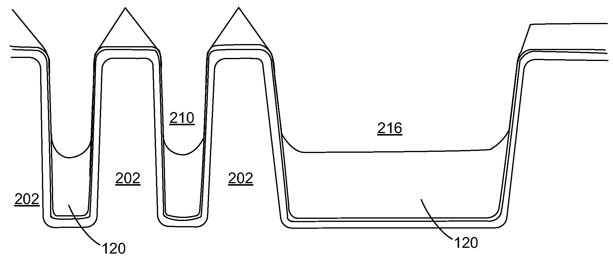
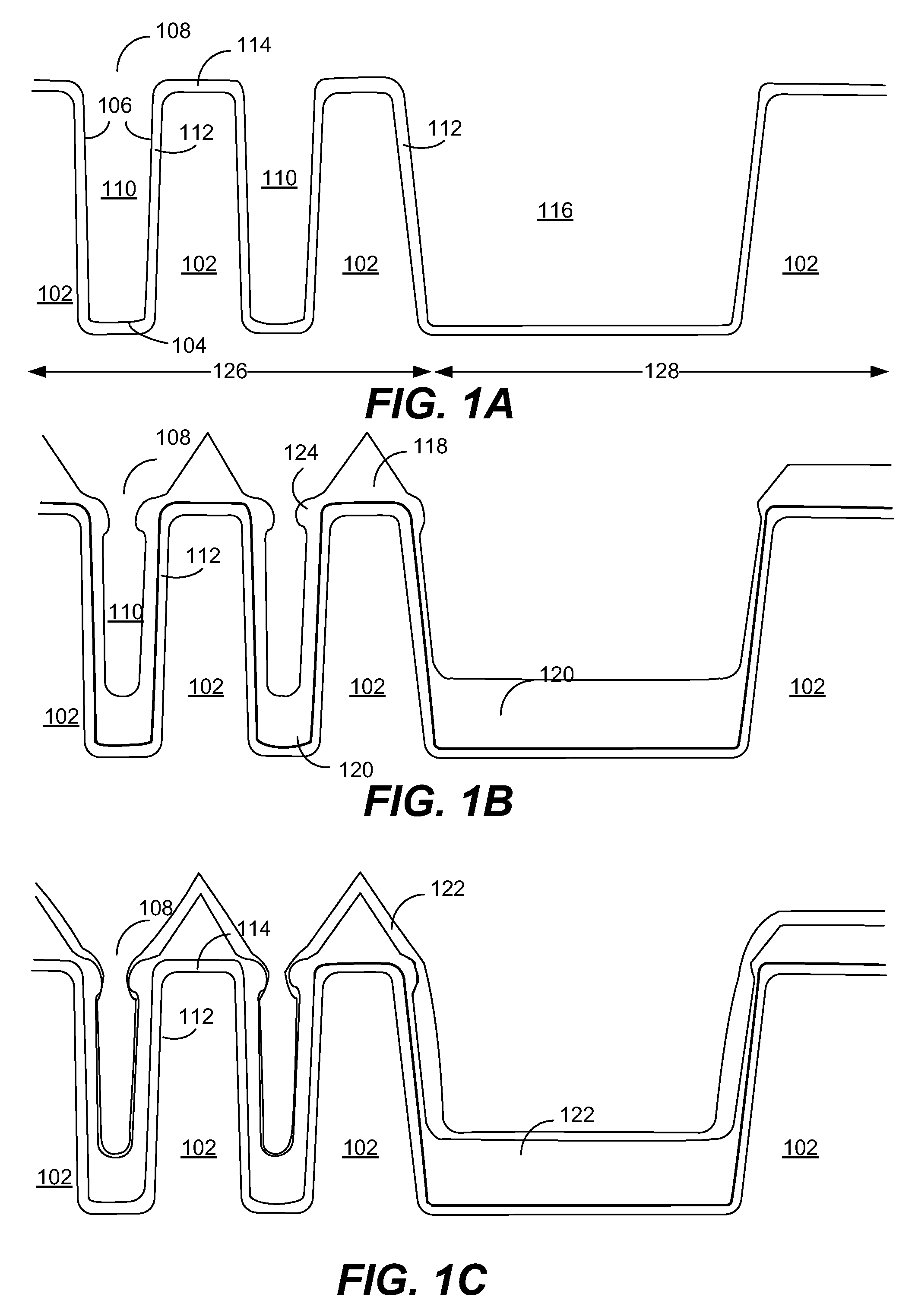
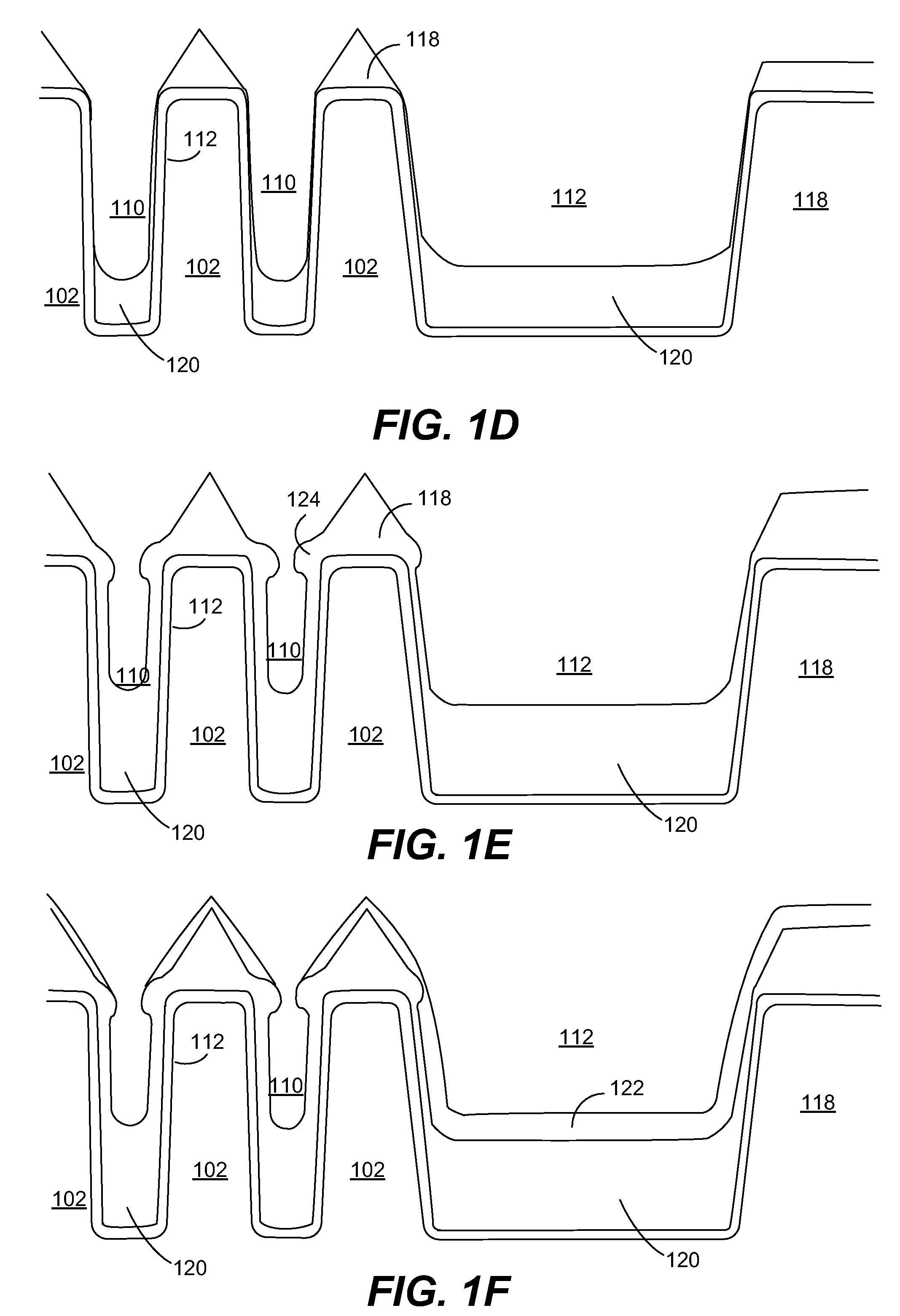
[0025]In the following detailed description of the present invention, a number of specific embodiments are set forth in order to provide a thorough understanding of the invention. While the invention will be described in conjunction with these specific embodiments, it will be understood that it is not intended to limit the invention to such specific embodiments. On the contrary, it is intended to cover alternatives, modifications, and equivalents as may be included within the spirit and scope of the invention as defined by the appended claims. In some descriptions herein, well-known processes, procedures, and components have not been described in detail so as not to unnecessarily obscure aspects of the present invention. For example, the present invention applies to a substrate having gaps in need of being filled by dielectric material. The invention is not, however, limited to such applications. It may be employed in a myriad of other fabrication processes such as for fabricating f...


PUM

PropertyMeasurementUnit
Fractionaaaaaaaaaa
Temperatureaaaaaaaaaa
Pressureaaaaaaaaaa

Abstract

In-situ semiconductor process that can fill high aspect ratio (typically at least 6:1, for example 7:1 or higher), narrow width (typically sub 0.13 micron, for example 0.1 micron or less) gaps without damaging underlying features and little or no incidence of voids or weak spots is provided. A protective layer is deposited to protect underlying features in regions of the substrate having lower feature density so that unwanted material may be removed from regions of the substrate having higher feature density. This protective layer may deposits thicker on a low density feature than on a high density feature and may be deposited using a PECVD process or low sputter/deposition ratio HDP CVD process. This protective layer may also be a metallic oxide layer that is resistant to fluorine etching, such as zirconium oxide (ZrO2) or aluminum oxide (Al2O3).

Description

FIELD OF THE INVENTION[0001]This invention relates to electronic device fabrication processes and associated apparatus. More specifically, the invention relates to chemical vapor deposition and dry etch processes for forming dielectric layers, particularly in substrates having high density and isolated feature regions.BACKGROUND OF THE INVENTION[0002]It is often necessary in semiconductor processing to fill high aspect ratio gaps with insulating material. This is the case for shallow trench isolation (STI), inter-metal dielectric (IMD) layers, inter-layer dielectric (ILD) layers, pre-metal dielectric (PMD) layers, passivation layers, etc. As device geometries shrink and thermal budgets are reduced, void-free filling of narrow width (e.g. less than 0.13 μm gap width), high aspect ratio (AR) features (e.g., AR>6:1) becomes increasingly difficult due to limitations of existing deposition processes.[0003]High density plasma (HDP) chemical vapor deposition (CVD), a directional (bottom...

Claims


Application Information

Patent Timeline
IPC IPC(8): H01L21/762
CPCC23C16/045H01L21/76801H01L21/76224C23C16/401H01L21/76H01L21/205H01L21/3065
Inventor VAN SCHRAVENDIJK, BARTHILL, RICHARD S.VAN DEN HOEK, WILBERTTE NIJENHUIS, HARALD
Owner NOVELLUS SYSTEMS
Why Eureka
Try Eureka