Compound semiconductor device

a semiconductor and compound technology, applied in the direction of semiconductor devices, basic electric elements, electrical apparatus, etc., can solve the problems of inability to stably manufacture, high photoelectric conversion efficiency, and subsequent growth of crystalline defects, so as to reduce the flow of device-operating current, high photoelectric conversion efficiency, and high intensity

Inactive Publication Date: 2009-12-17
SHOWA DENKO KK
View PDF2 Cites 17 Cited by
  • Summary
  • Abstract
  • Description
  • Claims
  • Application Information

AI Technical Summary

Benefits of technology

[0048]According to the eleventh aspect of this invention, since the (0.0.0.1.) crystal face constituting the compound semiconductor layer and the (0.0.0.1.) crystal face constituting the boron phosphide-based semiconductor layer are arranged parallel to the stacking direction of the compound semiconductor, the resistance to the flow of the device-operating current can be decreased. The eleventh aspect of this invention, therefore, brings an effect of enabling production of an LED exhibiting a high efficiency of photoelectric conversion and a high-frequency Field Effect Transistor (FET) suffering insignificantly from loss of electric power.
[0049]According to the twelfth aspect of this invention, since the boron phosphide-based semiconductor is formed of a hexagonal boron phosphide-based semiconductor containing no anti-phase boundary, for example, the product resulting from bonding this boron phosphide-based semiconductor to a compound semiconductor layer formed of a compound semiconductor can be effectively used as a material layer for disposing a hexagonal compound semiconductor layer containing no anti-phase boundary. Further, the twelfth aspect of this invention brings an effect of enabling a hexagonal compound semiconductor layer containing no anti-phase boundary to be utilized, for example, as a light-emitting layer and consequently allowing production of a semiconductor light-emitting device giving light emission of high intensity.
[0050]According to the thirteenth aspect of this invention, since the electrodes are so disposed that the device-operating current may flow in a direction substantially parallel to both the (0.0.0.1.) crystal face constituting the boron phosphide-based semiconductor layer and the (0.0.0.1.) crystal face constituting the compound semiconductor layer, the device-operating current can be made to flow more smoothly. The thirteenth aspect of this invention, therefore, brings an effect of enabling production of an LED having a small current in the forward direction, for example.
[0051]According to the fourteenth aspect of this invention, since the electrodes are so disposed that the device-operating current may be made to flow in a direction substantially perpendicular to both the (0.0.0.1.) crystal face constituting the boron phosphide-based semiconductor layer and the (0.0.0.1.) crystal face constituting the compound semiconductor layer, the device-operating current may be made to flow while encountering only small resistance. The fourteenth aspect of this invention, therefore, brings an effect of enabling production of a high-frequency power FET that suffers from only small loss of output due to heat generation.
[0052]According to the fifteenth aspect of this invention, since the boron phosphide-based semiconductor layer is formed of a hexagonal monomeric boron phosphide, the ohmic electrodes or the Schottky contac which incur or incurs only small current leakage can be conveniently formed by disposing the electrodes on the surface of a hexagonal monomeric boron phosphide layer containing crystalline defects in a particularly small density. The fifteenth aspect of this invention, therefore, brings an effect of enabling convenient provision of a light-emitting device having a high efficiency of photoelectric conversion or an FET furnished with a gate electrode of high breakdown voltage and endowed with an enhanced drain current pinch off property.
[0053]According to the sixteenth aspect of this invention, since the boron phosphide-based semiconductor layer is so formed of a hexagonal monomeric boron phosphide that the length of the c-axis of the boron phosphide may fall in the range between 0.52 nm or more and 0.53 nm or less, the layer (boron phosphide layer) formed of a hexagonal monomeric boron phosphide crystal containing crystalline defects, such as twins and stacking faults, only in a small amount can be produced. Further, the compound semiconductor layer of superior quality can be obtained by using the boron phosphide layer excelling in crystallinity. The sixteenth aspect of this invention, therefore, is capable of forming a compound semiconductor device with a boron phosphide-based semiconductor layer excelling in crystallinity and consequently bringing an effect of enhancing the characteristic properties of the compound semiconductor device.

Problems solved by technology

Even when a substrate is formed of silicon and a boron phosphide-based semiconductor layer is grown on the surface formed of a (111) crystal face of the substrate, however, the layer consequently grown eventually contains crystalline defects, such as stacking faults and twins, in a large amount (T. Udagawa and G. Shimaoka, J. Ceramic Processing Res., (Republic of Korea), Vol. 4, No. 2, 2003, pp.
Even when using the stacked structure that is provided with the boron phosphide-based semiconductor layer containing such crystalline defects in a large amount, for example, there is the problem that the LED possessing high voltage in the reverse direction and manifesting a high efficiency in photoelectric conversion, for example, cannot be stably manufactured.
Even when using the Group III nitride semiconductor layer containing crystalline defects, such as dislocations, in a large amount for a functional layer, such as a light-emitting layer, there is the problem that the produced LED will not be enabled to increase the voltage in the reverse direction or to enhance the efficiency of photoelectric conversion.
Furthermore, for example, the configuration of the FET by utilizing as an electron transporting layer (channel layer) the Group III nitride semiconductor layer containing crystalline defects in a large amount entails the problem that the high-frequency properties, such as power output, will not be enhanced fully satisfactorily because of the failure to acquire high electron mobility.
Heretofore, the compound semiconductor devices have not been always manufactured by utilizing semiconductor layers of superior quality excelling in crystallinity.
The boron phosphide-based crystal layer and the Group III nitride semiconductor layer which contain the anti-phase boundaries in a large amount and reveal inferior crystallinity hinder the effort to obtain the LED excelling in efficiency of light emission and the FET excelling in electrical properties with sufficient stability.
Even when the ohmic electrodes are disposed contiguously to a cubic boron phosphide-based semiconductor layer containing crystalline defects in a large amount, they entail the problem that the LED possessing a high voltage in the reverse direction and manifesting a high efficiency of photoelectric conversion will not be stably manufactured because the operating current for operating the device (device-operating current) incurs desirable leakage via crystalline defects, such as twins.
Even when Schottky contact is disposed on the surface of a cubic boron phosphide-based semiconductor layer abounding in crystalline defects, they entail the problem that the FET excelling in high-frequency properties will not be stably produced because the gate electrode suffering from great leakage current and deficient breakdown voltage is formed eventually and the drain current manifests an inferior pinch-off property.
The layer in question, for example, entails the problem that, owing to the mismatching of lattice with the under layer, it will eventually become a crystalline layer containing plane defects, such as twins and stacking faults copiously.
When the light-emitting part of the LED is manufactured by using as the clad layer, for example, the boron phosphide-based semiconductor layer copiously containing such crystalline defects, no success has yet been achieved in producing stably the LED of high luminance because the occurrence of the short-circuit flow of the current for operating the LED to the light-emitting layer prevents the surface area for light emission from being expanded.

Method used


Image

  • Compound semiconductor device
  • Compound semiconductor device
  • Compound semiconductor device

Examples


example 1

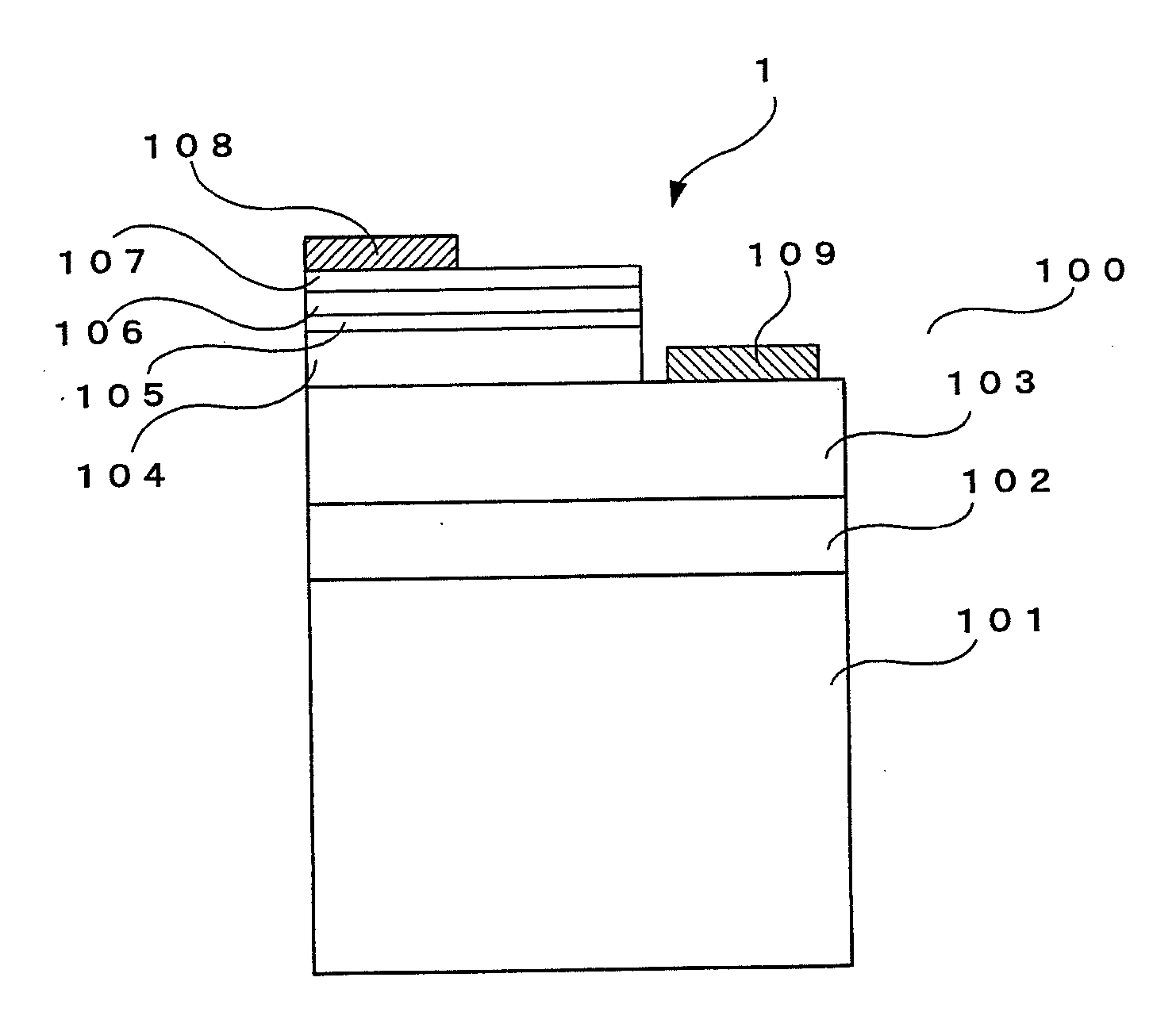
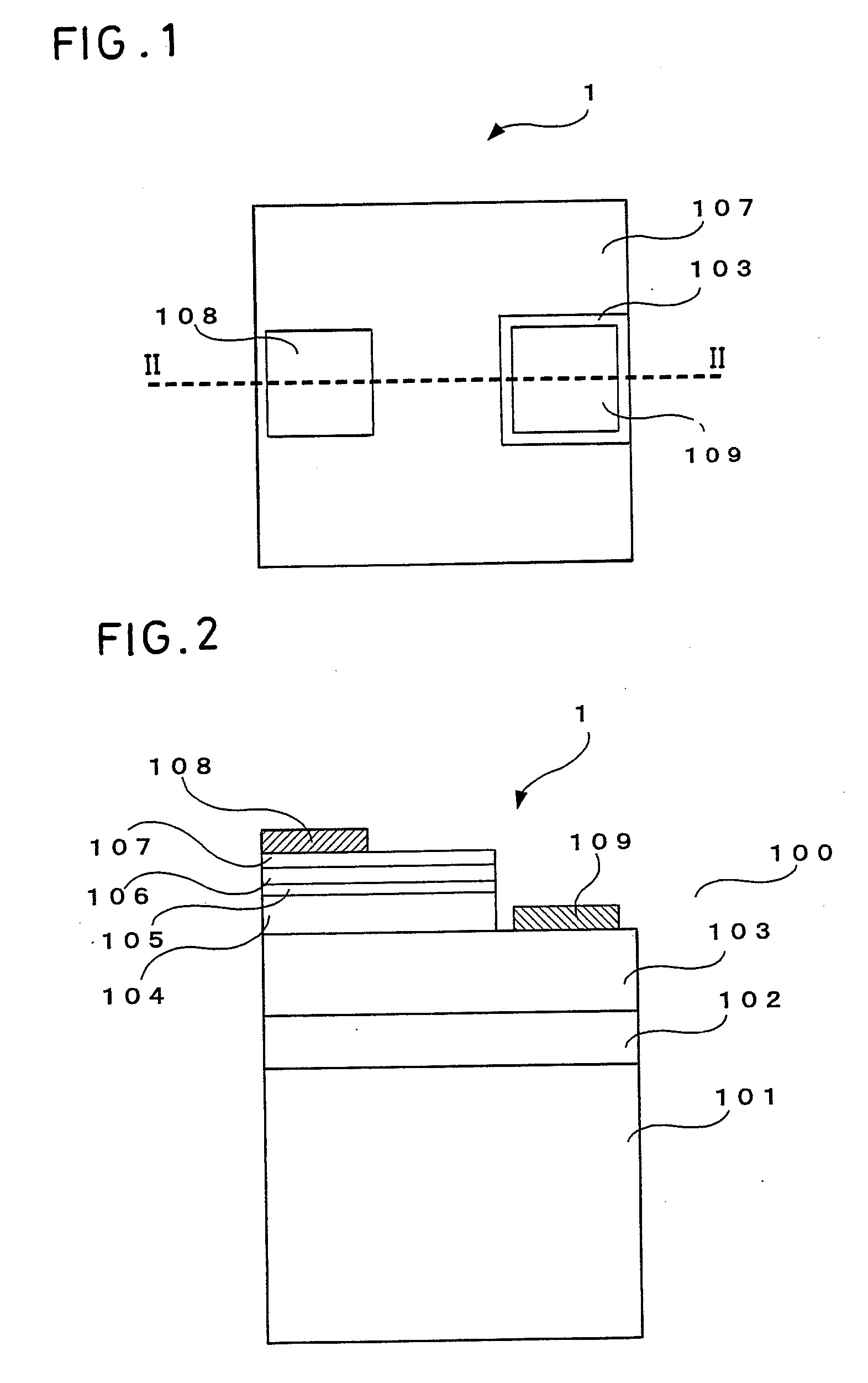
[0189]This invention will be specifically explained by citing as an example the case of configuring a compound semiconductor LED by utilizing a hexagonal monomeric BP layer disposed as bonded on the surface formed of a (1.1.-2.0.) crystal face of a bulk crystal of sapphire.

[0190]FIG. 1 schematically illustrates the planar structure of the LED to which this Example 1 pertains. Then, FIG. 2 is a schematic cross section illustrating the compound semiconductor device LED 1, taken through FIG. 1 along the broken line II-II.

[0191]A stacked structure 100 intended to manufacture the LED 1 was formed by using as a substrate 101 a sapphire (α-alumina single crystal) having a (1.1.-2.0.) crystal face (commonly called “A-plane”) as its surface. On the surface of the (1.1.-2.0.) crystal face of the substrate 101, an undoped n-type hexagonal monomeric BP layer formed in a thickness of about 290 nm was formed as a hexagonal boron phosphide-based semiconductor layer 102 by using the ordinary MOCVD ...

example 2

[0197]The contents of this invention will be specifically explained by citing as an example the case of configuring a compound semiconductor LED by adopting a bulk crystal of sapphire as a hexagonal single crystal and utilizing a hexagonal monomeric BP layer disposed thereon.

[0198]FIG. 8 schematically illustrates the planar structure of a LED to which this Example 2 pertains. Then, FIG. 9 is a schematic cross section illustrating the LED 1 taken through FIG. 8 along the broken line IX-IX.

[0199]The stacked structure 100 intended for manufacture of the LED 1 was formed by using as the substrate 101 a sapphire having a (1.1.-2.0.) crystal face as its surface. On the surface of the substrate 101, the undoped n-type hexagonal monomeric BP layer 102 having a layer thickness of about 290 nm was formed by using an ordinary MOCVD method.

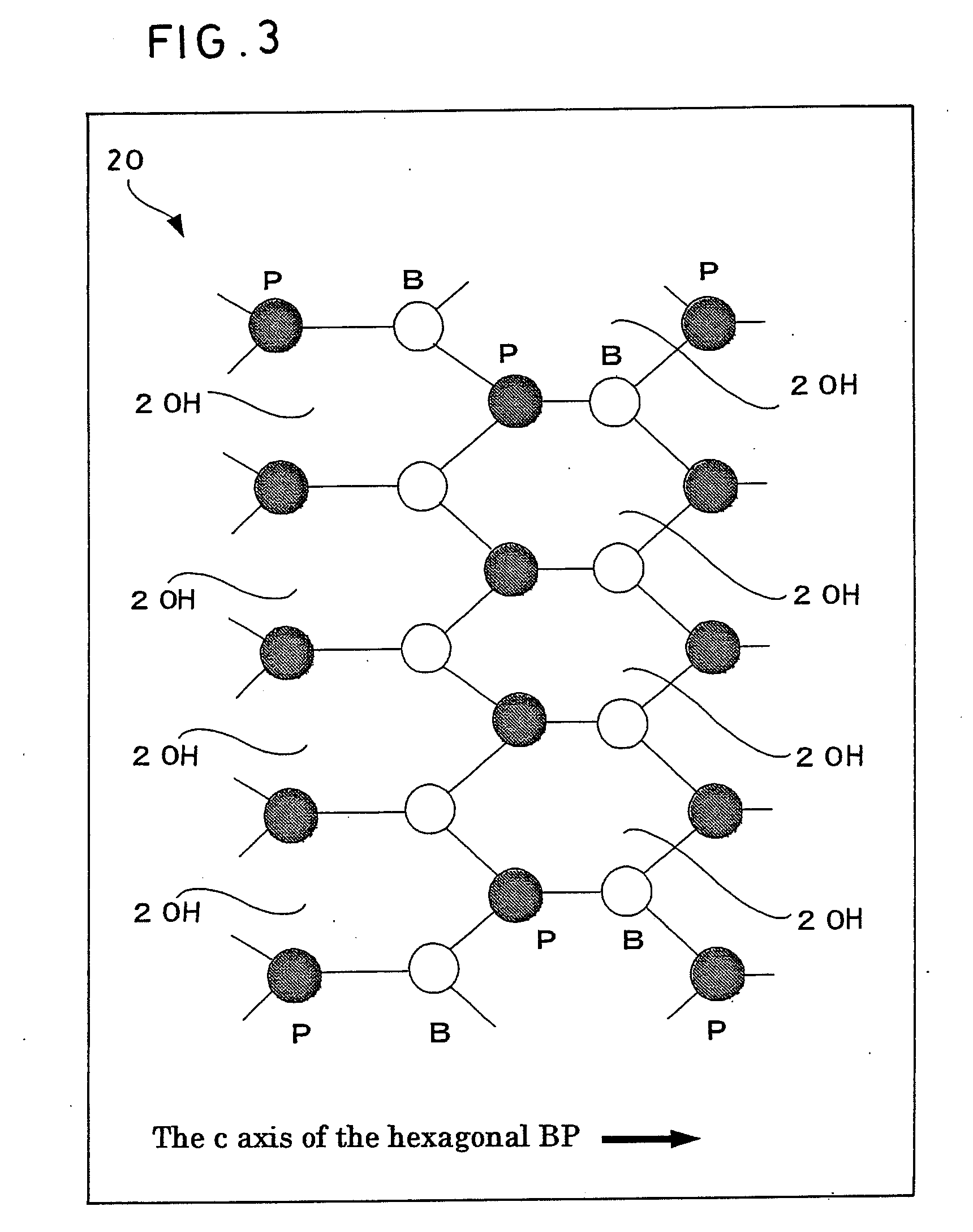
[0200]By an ordinary TEM analysis, the (0.0.0.1.) crystal face of the hexagonal monomeric BP layer 102 was shown to be arranged in a mutually parallel state ...

example 3

[0206]This invention will be specifically explained by citing as an example the case of configuring a compound semiconductor LED from a stacked structure provided with a GaN layer having a (1.1.-2.0.) crystal face as its surface and a hexagonal monomeric BP layer disposed as bonded to the surface and having a (1.1.-2.0.) crystal face as its surface.

[0207]FIG. 10 schematically illustrates the planar structure of the LED 1 to which this Example 3 pertains. FIG. 11 is a schematic cross section illustrating the LED 1 taken through FIG. 10 along broken line XI-XI.

[0208]The stacked structure 100 intended to manufacture the LED 1 was formed by using as a substrate 101a sapphire (α-alumina single crystal) having a (1.-1.0.2.) crystal face (commonly called R-plane) as its surface. On the surface of the (1.-1.0.2.) crystal face of the substrate 101, an undoped n-type GaN layer 103 having a (1.1.-2.0.) crystal face as its surface was formed by utilizing an ordinary MBE method. The dislocation ...


PUM


Abstract

A compound semiconductor device (1) includes a compound semiconductor having a stacked structure (100) of a hexagonal single crystal layer (101), a boron phosphide-based semiconductor layer (102) formed on a surface of the hexagonal single crystal layer and a compound semiconductor layer (103) disposed on the boron phosphide-based semiconductor layer, and electrodes (108, 109) disposed on the stacked structure, wherein the boron phosphide-based semiconductor layer is formed of a hexagonal crystal disposed on a surface formed of a (1.1.-2.0.) crystal face of the hexagonal single crystal layer.

Description

CROSS REFERENCE TO RELATED APPLICATIONS[0001]This application is an application filed under 35 U.S.C. §111(a) claiming the benefit pursuant to 35 U.S.C. §119(e)(1) of the filing dates of Provisional Applications No. 60 / 717,759 filed Sep. 19, 2005, No. 60 / 718,331 filed Sep. 20, 2005, No. 60 / 720,482 filed Sep. 27, 2005, No. 60 / 721,592 filed Sep. 29, 2005, No. 60 / 722,423 filed Oct. 3, 2005, No. 60 / 725,323 filed Oct. 12, 2005 and No. 60 / 734,316 filed Oct. 27, 2005 and Japanese Patent Applications No. 2005-259042 filed Sep. 7, 2005, No. 2005-261946 filed Sep. 9, 2005, No. 2005-266418 filed Sep. 14, 2005, No. 2005-269516 filed Sep. 16, 2005, No. 2005-277536 filed Sep. 26, 2005, No. 2005-286495 filed Sep. 30, 2005 and No. 2005-312758 filed Oct. 27, 2005 pursuant to 35 U.S.C. §111(b).TECHNICAL FIELD[0002]This invention relates to a compound semiconductor device configured by having electrodes disposed on a stacked structure provided with a hexagonal single crystal, a boron phosphide-based s...

Claims


Application Information

Patent Timeline
Patent Type & Authority Applications(United States)
IPC IPC(8): H01L29/02
CPCH01L29/045H01L29/2003H01L33/30H01L33/16H01L29/7787
Inventor UDAGAWA, TAKASHI
Owner SHOWA DENKO KK
Why Eureka
Try Eureka