
Method of forming high-k dielectric films based on novel titanium, zirconium, and hafnium precursors and their use for semiconductor manufacturing

a technology of zirconium and hafnium, which is applied in the direction of metal/alloy conductors, organic chemistry, and conductors, etc., can solve the problems of affecting the final properties of the surface/interface, affecting the final properties of the product, and other possible byproducts, depending on the oxygen source used, to achieve the effect of not enabling self-limited deposition in the ald process

Active Publication Date: 2009-12-17
LAIR LIQUIDE SA POUR LETUDE & LEXPLOITATION DES PROCEDES GEORGES CLAUDE
View PDF25 Cites 84 Cited by
  • Summary
  • Abstract
  • Description
  • Claims
  • Application Information

AI Technical Summary

Benefits of technology

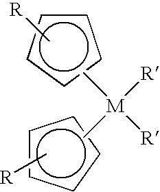
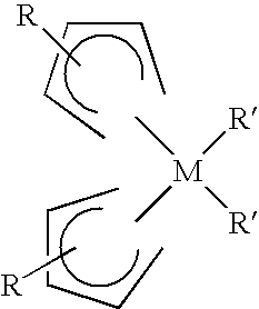
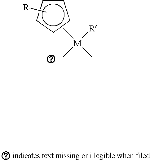
The invention provides a method for depositing thin films of metal-containing materials using certain cyclopentadienyl or pentadienyl based precursors that are liquid at room temperature. These precursors have the advantage of being thermally stable, meaning they can be distributed without generating particles. The method allows for the deposition of a variety of Group IV metals, including titanium, zirconium, and hafnium. The method can be used to form films containing a variety of elements, such as oxygen, nitrogen, and silicon. The method can be carried out using a reactor and a co-reactant, such as H2O, NH3, or BDMA. The resulting films have good thermal stability and can be used for various applications such as semiconductor devices and optical components.

Problems solved by technology

However, some by-products generated during the deposition process, such as HCl or Cl2, can cause surface / interface roughness that can be detrimental to the final properties.
Other possible byproducts, depending on the oxygen source used, may be hazardous.
Moreover, in the case of high-k oxide, Cl or F impurities are detrimental to the final electrical properties and Cl and F-containing precursors are therefore not preferred.
However, all those alkoxide precursors have the drawback not to enable self-limited deposition in ALD process.
esses. Furthermore, some are liquid at room temperature (TDEAH and TEMAH) and of sufficient volatility, and they allow self-limited ALD at low temperature for a limited thermal budget p
rocess. However, Group IV alkylamides have several drawbacks:they may decompose during the distribution to some extent leading to a possible clogging of the feeding line or the vaporizer,they may generate particles during deposition,they may entail non-uniform compositions during deep trenches deposition processes,they only allow a narrow self-limited ALD temperature window, hence reducing the process window.< /
However, HfCp2Me2 and ZrCp2Me2 both have the drawback of being solid products at room temperature (HfCp2Me2 melting point is 57.5° C.).
This makes inconvenient their use by IC makers.

Method used


Image

  • Method of forming high-k dielectric films based on novel titanium, zirconium, and hafnium precursors and their use for semiconductor manufacturing
  • Method of forming high-k dielectric films based on novel titanium, zirconium, and hafnium precursors and their use for semiconductor manufacturing
  • Method of forming high-k dielectric films based on novel titanium, zirconium, and hafnium precursors and their use for semiconductor manufacturing

Examples


example i

Deposition of Metal Oxide Film M1O2 with M1 being Preferably Hafnium and Zirconium

[0083]The film to be deposited relates to the case where a=0, b is about 2 and c=0.

[0084]To make the deposition of such film on the surface of a wafer or in a deep trench to manufacture MIM structures for DRAM, one need to vaporize the M1 metal source as defined in steps (b) and / or (h) here above into the reactor (preferably Hafnium or Zirconium), inject an oxygen source, preferably moisture, oxygen or ozone into said reactor, react the products at appropriate temperature (preferably between 150° C. and 350° C.) and pressure (preferably between 25 Pa and 1000 Pa) for the duration necessary to achieve either a thin film deposition on the substrate or to fill out deep trenches by ALD or pulse CVD process (sequential pulse injection of metal sources are necessary in order to allow regular deposition of the oxide in the trench to progressively fill out this trench and provide no voids in the dielectric fil...

example ii

Deposition of Metal Oxynitride Films M1ON with M1 being Preferably Hafnium and Zirconium

[0116]The film deposited relates to the case where a=0 and b and c are different from zero.

[0117]All the information given in Example I is applicable in this Example II, except that nitrogen needs to be introduced into the reactor.

[0118]The nitrogen shall be selected from a nitrogen source selected from the group comprising nitrogen (N2), ammonia, hydrazine and alkyl derivatives, N-containing radicals (for instance N., NH., NH2.), NO, N2O, NO2 or the like.

example iii

Deposition of M1M2 Metal Oxide Films with M1 being Preferably Hf or Zr and M2 being Preferably Si or Al

[0119]The film deposited on the substrate in this example illustrates the case wherein a≠0, b≠0 and c=0.

[0120]All the information given in Example I are applicable in this Example III, except that a M2 metal source is additionally needed.

[0121]The M2 containing precursor is also introduced into the reactor to crate the M2 source of metal. This M2 containing precursor source shall be preferably:

a) a silicon (or germanium) source and is selected from, but not limited to, the group consisting of disiloxane, trisilylamine, disilane, trisilane, a alkoxysilane SiHx(OR1)4-x, a silanol Si(OH)x(OR1)4-x (preferably Si(OH)(OR1)3; more preferably Si(OH)(OtBu)3 an aminosilane SiHx(NR1R2)4-x (where x is comprised between 0 and 4; R1 and R2 are independently H or a C1-C6 carbon chain, either linear, branched or cyclic; preferably TriDMAS SiH(NMe2)3; BTBAS SiH2(NHtBu)2) BDEAS SiH2(NEt2)2) and mixt...


PUM

PropertyMeasurementUnit
temperatureaaaaaaaaaa

Abstract

A method of forming on at least one support at least one metal containing dielectric films having the formula (M11-a M2a) Ob Nc, wherein: 0≦a<1, 01 and M2 being metals Hf, Zr or Ti using precursors with pentadienyl ligands and / or cyclopentadienyl ligands.

Description

[0001]The invention relates to a method of forming high-k dielectric films such as hafnium or zirconium oxides or oxynitrides and their use for manufacturing semi-conductors.BACKGROUND[0002]With the shrink of the critical dimensions of the future generation of semi-conductor devices, the introduction of new materials, especially having high dielectric constant, is required. In CMOS architectures, high-k dielectrics are required to replace SiO2 which reaches its physical limits, having typically a SiO2 equivalent thickness of about 1 nm.[0003]Similarly, high-k dielectrics are required in Metal-Insulator-Metal architectures for RAM applications. Various metal compositions have been considered to fulfill both the materials requirements (dielectric constant, leakage current, crystallisation temperature, charge trapping) and the integration requirements (thermal stability at the interface, dry etching feasibility . . . ).[0004]The Group IV based materials, such as HfO2, HfSiO4, ZrO2, ZrS...

Claims


Application Information

Patent Timeline
Patent Type & Authority Applications(United States)
IPC IPC(8): H01L21/316H01B1/02
CPCC23C16/18C23C16/308C23C16/34C23C16/405C07F17/00H01L21/31641H01L21/31645C07F7/00C07F7/006H01L21/3141H01L21/02148H01L21/02159H01L21/02178H01L21/02181H01L21/02189H01L21/02194H01L21/0228C23C16/40C07F7/003H01L21/02205H01L21/02271H01L21/02192H01L21/67207H01L21/8238H01L21/0262C23C16/45553H01L21/02216H01L21/02211C23C16/403C23C16/407
Inventor BLASCO, NICOLASDUSSARRAT, CHRISTIAN
Owner LAIR LIQUIDE SA POUR LETUDE & LEXPLOITATION DES PROCEDES GEORGES CLAUDE
Learn More