High-q disk NANO resonator device and method of fabricating the same

a nano-resonator and nano-resonator technology, applied in the field of micro-mechanical resonators, can solve the problems of increasing losses, reducing q, and large air damping losses, and achieves the effects of reducing air damping losses, minimizing elastic wave radiation, and high quality factor

Inactive Publication Date: 2009-12-24
HONEYWELL INT INC
View PDF13 Cites 14 Cited by
  • Summary
  • Abstract
  • Description
  • Claims
  • Application Information

AI Technical Summary

Benefits of technology

[0010]The nano structure can be patterned in a polymethylmethacrylate (PMMA) film or a ZEP film utilizing an electron beam lithography process. The nanoresonator comprises a disk structure or a ring structure with high quality factor and a diameter of sub micron or micron size. The high-Q nano structures can be fabricated utilizing nano fabrication tools such as E-beam lithography or focused ion beam (FIB) etching on conductive and insulating layers associated with a wafer. Anchor beams can provide electrical contact to the nanoresonator. The nanoresonator can be electrostatically driven into its radial contour resonant modes by the input electrodes. The small radial expansion and contraction amplitudes in the resonant modes greatly reduce the air damping and the motionless anchor beams minimize elastic wave radiation. Such nanoresonator device can provide significant advantages of multiple times or order of magnitude of higher sensitivity, higher frequency, lower power, and higher density.

Problems solved by technology

The problem associated with the development of such nanoresonator (ex., nanowire resonator) is due to the reliable low-loss structure and fabrication.
Also, such nanoresonator often results in large air damping losses and anchor losses that affects Q. In addition to anchor losses, air-damping forces create more losses when operating in atmosphere and hence further reduction in Q. Low-loss microresonator structures have been demonstrated using MEMS processes.
However, it is not easy to fabricate a low-loss structure in 1 um or sub micron size utilizing prior art fabrication process because of the smaller size and multiple sub-micron-alignment needs.

Method used


Image

  • High-q disk NANO resonator device and method of fabricating the same
  • High-q disk NANO resonator device and method of fabricating the same
  • High-q disk NANO resonator device and method of fabricating the same

Examples


Embodiment Construction

[0017]The particular values and configurations discussed in these non-limiting examples can be varied and are cited merely to illustrate at least one embodiment and are not intended to limit the scope thereof.

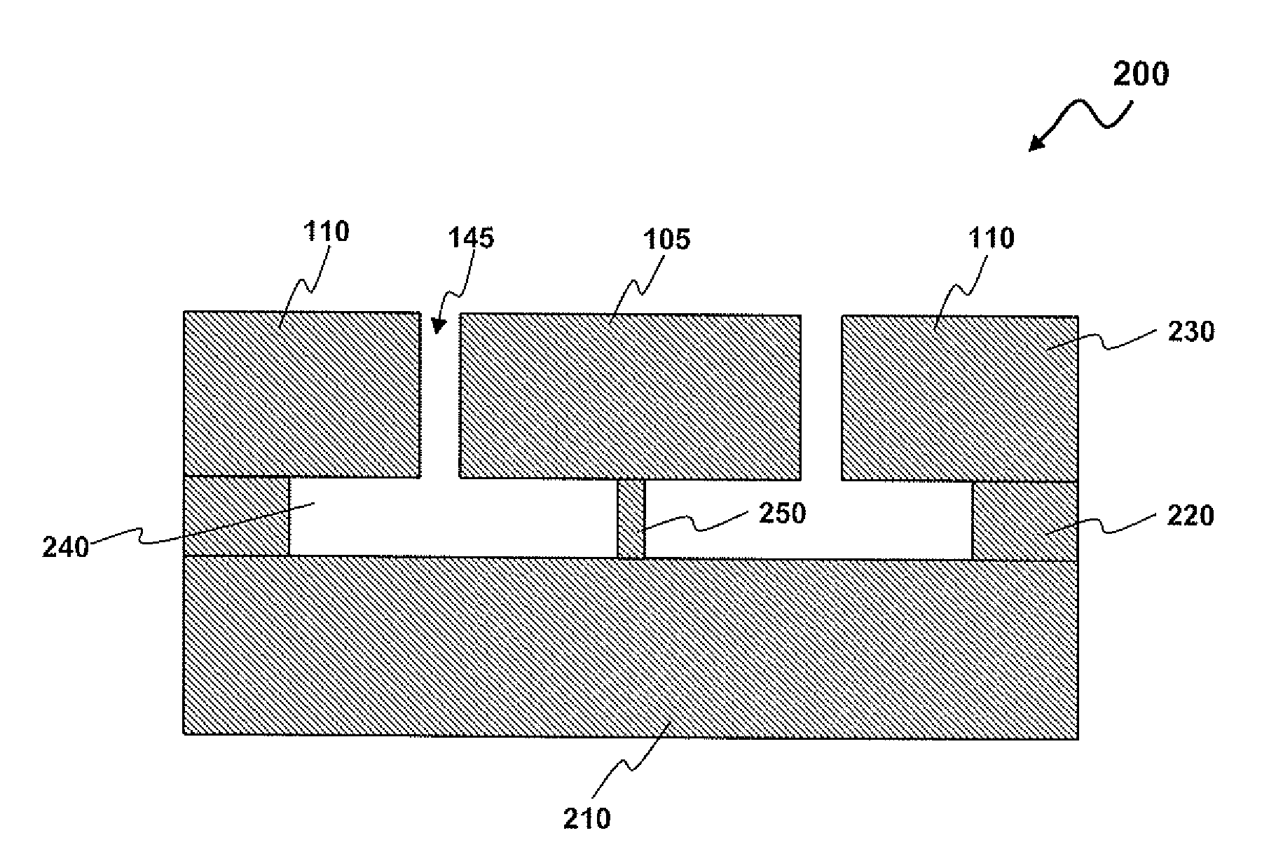
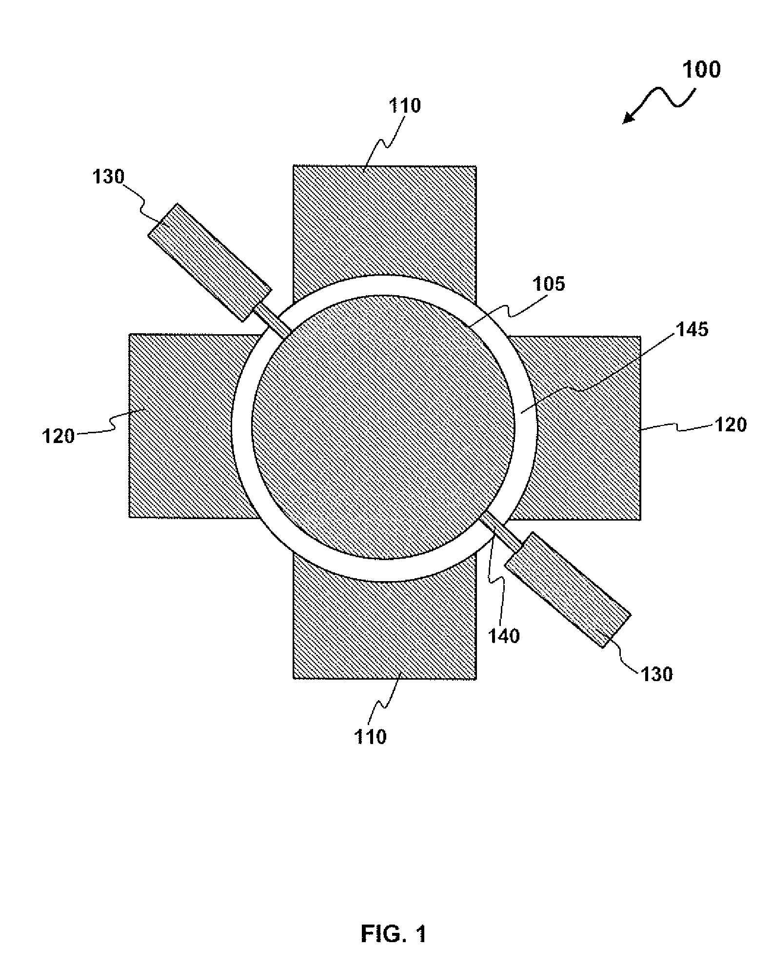
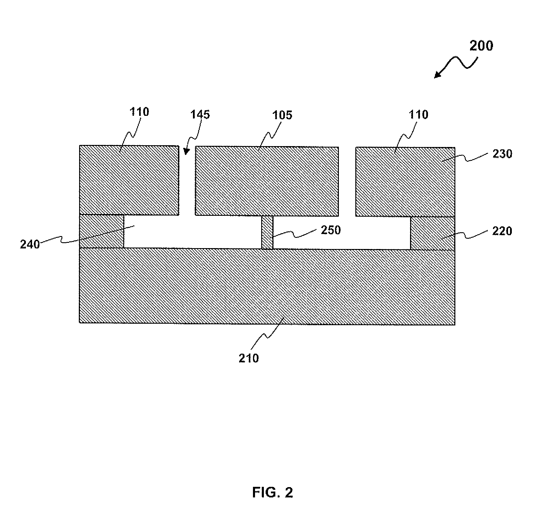
[0018]Referring to the drawings and in particular to FIG. 1, there is depicted a top view of a high-Q disk nanoresonator device 100, in accordance with a preferred embodiment. The nano disk resonator device 100 generally includes an input electrode 110 and an output electrode 120. Electrodes 110 and 120 can be symmetrical and interchangeable. The device 100 can further include a resonator disk 105 anchored at its motionless nodal points of its resonance modes by an anchor 130 supported by a support beam 140. The nano features for the high-Q nano disk resonator device 100 can be incorporated by the resonator disk 105 having a diameter of approximately 100-5000 nm and a thickness of approximately 200-400 nm. An air gap 145 spacing the input electrode 110 and the output electrode ...


PUM


Abstract

A nanoresonator device with high quality factor and method for fabricating the same is disclosed herein. The nanoresonator device generally includes an input electrode, an output electrode, a nanoresonator anchored at its motionless nodal points of its resonance modes by support beam(s) and/or anchor. The nanoresonator device can be fabricated on various wafers including a silicon on insulator (SOI) wafer, which includes an insulating layer and a heavily doped silicon layer. The nano structures with high quality factor can be patterned on a film utilizing nano fabrication tools and the patterned structures can be utilized as a mask to form permanent nano structures on the silicon layer by reactive ion etching (RIE). The insulating layer can be removed to form the anchor beams and a cavity by wet etching utilizing an etching solution.

Description

TECHNICAL FIELD[0001]Embodiments are generally related to micromechanical resonators. Embodiments are also related to nanoresonators. Embodiments are additionally related to methods for fabricating nanoresonators.BACKGROUND OF THE INVENTION[0002]Microelectromechanical systems (MEMS) include mechanical and electrical components having dimensions in the order of microns or smaller. MEMS structures can be utilized in numerous applications including microsensors and microresonators. Micromechanical resonators have been widely studied for RF signal processing (e.g., oscillator, filter, and mechanical circuit) and for high-precision measurements (e.g., mass / chemical, force, position, and frequency). Vibrating RF MEMS resonators are widely studied for frequency selection in communication sub-systems because of their high quality factor (Q) and excellent stability against thermal variations and aging. Vibrating RF MEMS resonators can replace off-chip components and improve the system size, ...

Claims


Application Information

Patent Timeline
Patent Type & Authority Applications(United States)
IPC IPC(8): H03H9/00H01L21/00
CPCH03H2009/0237H03H9/2436
Inventor SHEEDY, SABRINA C.DETRY, JAMES F.PECZALSKI, ANDRZEJZHANG, CHUNBOEICKHOFF, STEVEN J.
Owner HONEYWELL INT INC
Why Eureka
Try Eureka