TFT floating gate memory cell structures

a memory cell and floating gate technology, applied in the field of integrated circuits, can solve the problems of difficult reducing memory devices, difficult devices, and high cost of ic fabrication facilities, and achieve the effects of high field effect mobility, small geometric cell size and layered structure, and high reliability of cvd

Active Publication Date: 2010-01-07
SEMICON MFG INT (SHANGHAI) CORP +1
View PDF8 Cites 215 Cited by
  • Summary
  • Abstract
  • Description
  • Claims
  • Application Information

AI Technical Summary

Benefits of technology

[0011]Many benefits can be achieved by way of the present invention over conventional techniques. According to certain embodiments, the present invention combines the advantages of high reliability of CVD silicon floating gate for charge-trapping, small geometric cell size and layered structure, high field effect mobility using a polysilicon thin-film transistor as the access device, and low thermal budget for fabrication and dopant activation within temperature ranges tolerated by the memory cell. In addition, the present invention provides a simple process that is compatible wit...

Problems solved by technology

An IC fabrication facility can cost hundreds of millions, or even billions, of dollars.
Making devices smaller is very challenging, as each process used in IC fabrication has a limit.
Over the past, reducing memory devices have been a challenging task.
As an ex...

Method used


Image

  • TFT floating gate memory cell structures
  • TFT floating gate memory cell structures
  • TFT floating gate memory cell structures

Examples


Embodiment Construction

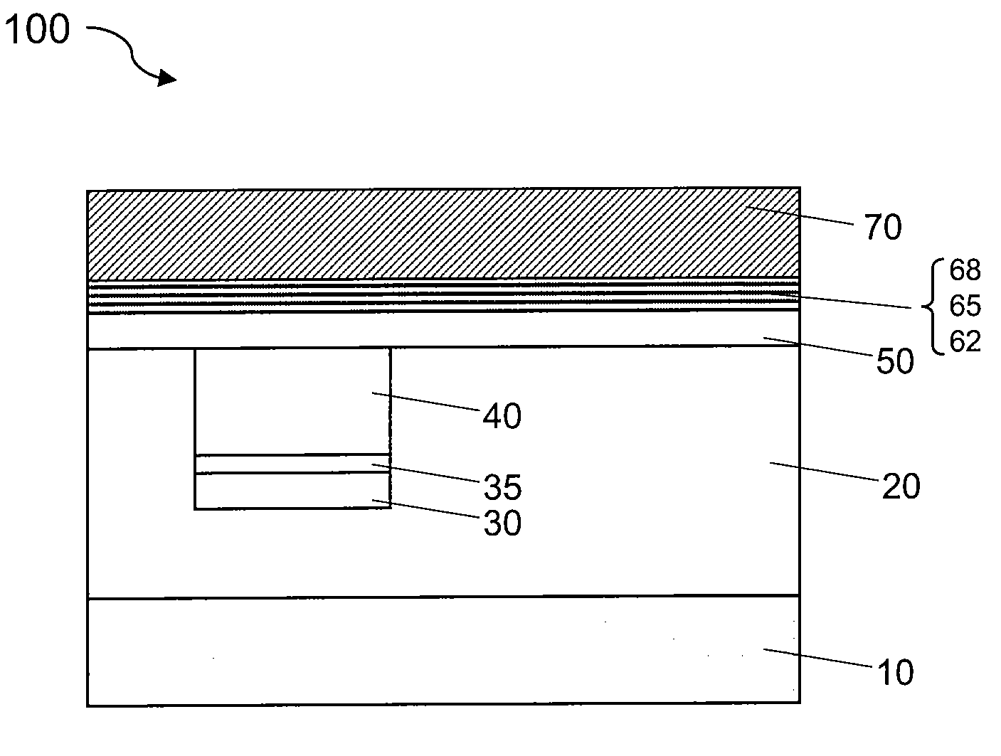
[0024]The present invention is directed to integrated circuits and their processing for the manufacture of semiconductor devices. More particularly, the invention provides a method for making semiconductor device having a memory cell. Merely by way of example, the invention has been applied to a thin film transistor (TFT) memory cell structure including a floating gate and a method for making the same cell structure and forming three-dimensional array. But it would be recognized that the invention has a much broader range of applicability. For example, the invention can be applied to a variety of devices having a control gate and a floating gate as memory storage element, such as dynamic random access memory devices, static random access memory devices, flash memory devices, and others.

[0025]As discuss above, various conventional techniques have been directed to memory cells with reduced sizes. According to one of the conventional techniques, memory cells are implemented with stacke...


PUM


Abstract

A device having thin-film transistor (TFT) floating gate memory cell structures is provided. The device includes a substrate, a dielectric layer on the substrate, and one or more source or drain regions being embedded in the dielectric layer. the dielectric layer being associated with a first surface. Each of the one or more source or drain regions includes an N+ polysilicon layer on a diffusion barrier layer which is on a first conductive layer. The N+ polysilicon layer has a second surface substantially co-planar with the first surface. Additionally, the device includes a P polysilicon layer overlying the co-planar surface and a floating gate on the P polysilicon layer. The floating gate is a low-pressure CVD-deposited silicon layer sandwiched by a bottom oxide tunnel layer and an upper oxide block layer. Moreover, the device includes at least one control gate made of a P+ polysilicon layer overlying the upper oxide block layer. A method of making the same memory cell structure is provided and can be repeated to integrate the structure three-dimensionally.

Description

CROSS-REFERENCE TO RELATED APPLICATIONS[0001]This application claims priority to Chinese Patent Application No. 200810040295.X, filed Jul. 3, 2008, commonly assigned, and incorporated herein by reference for all purposes.BACKGROUND OF THE INVENTION[0002]The present invention is directed to integrated circuits and their processing for the manufacture of semiconductor devices. More particularly, the invention provides a method for making semiconductor device having a memory cell. Merely by way of example, the invention has been applied to a thin film transistor (TFT) memory cell structure including a floating gate and a method for making the same cell structure and forming three-dimensional array. But it would be recognized that the invention has a much broader range of applicability. For example, the invention can be applied to a variety of devices having a control gate and a floating gate as memory storage element, such as dynamic random access memory devices, static random access m...

Claims


Application Information

Patent Timeline
IPC IPC(8): H01L29/788H01L21/84
CPCH01L29/66757H01L29/788H01L29/7881H01L29/66825
Inventor MIENO, FUMITAKE
Owner SEMICON MFG INT (SHANGHAI) CORP
Why Eureka
Try Eureka