The resolution of a lithographic image is limited by the wavelength of the light that forms it.
However, evanescent
waves can only exist in extremely thin films, and even the somewhat larger thicknesses that are typically given to photoresist films (of order 0.1-1.0 microns) are microscopic on the scale of the lens elements which propagate the light from
mask to
wafer.
The macroscopic size of conventional projection lenses makes them unsuitable for exploiting waves that become evanescent in any medium between the
resist film stack and the
mask.
In fact, until recently, lithographic projection lenses were incapable of introducing spatial frequencies into the image that corresponded to wavelengths shorter than the vacuum wavelength.
Moreover, the lens elements in 193 nm systems also face stringent materials requirements, and their
refractive index is currently limited to n=1.56 or below.
This is because the final lens element generally cannot have a concave
exit surface since the immersion cavity would then become impractically thick along the
optical axis, greatly stiffening the already difficult-to-surmount materials requirements that a hypothetical high-index immersion fluid must meet.
In fact, it is currently believed that the materials challenges involved in significantly raising the
refractive index of the final lens element are at least as difficult as those faced in raising the index of the
coupling medium.
Achieving the necessary freedom from minute levels of index in-homogeneity and uncorrectable
birefringence is extremely difficult at 193 nm, given the element sizes and tolerance levels needed for advanced
lithography lenses.
Unfortunately, even with one dimensional (1D) layouts, the tight transfer
process control needed to print a narrow feature from a wide image will usually prevent a doubling of minimum manufacturable resolution from being feasible by this means—resolution improvements are typically quite a bit less than 2×.
Even under ideal conditions, achievement of more than a doubling of resolution would require three or more transfer steps, which would cause cost to rise very substantially.
Note that with two-dimensional (2D) patterns, a fill doubling of resolution in every cross-section (e.g. along both the x and y axes) is not even theoretically possible if only two exposures are used.
However, this classic approach is inherently unable to provide more than a single doubling of resolution.
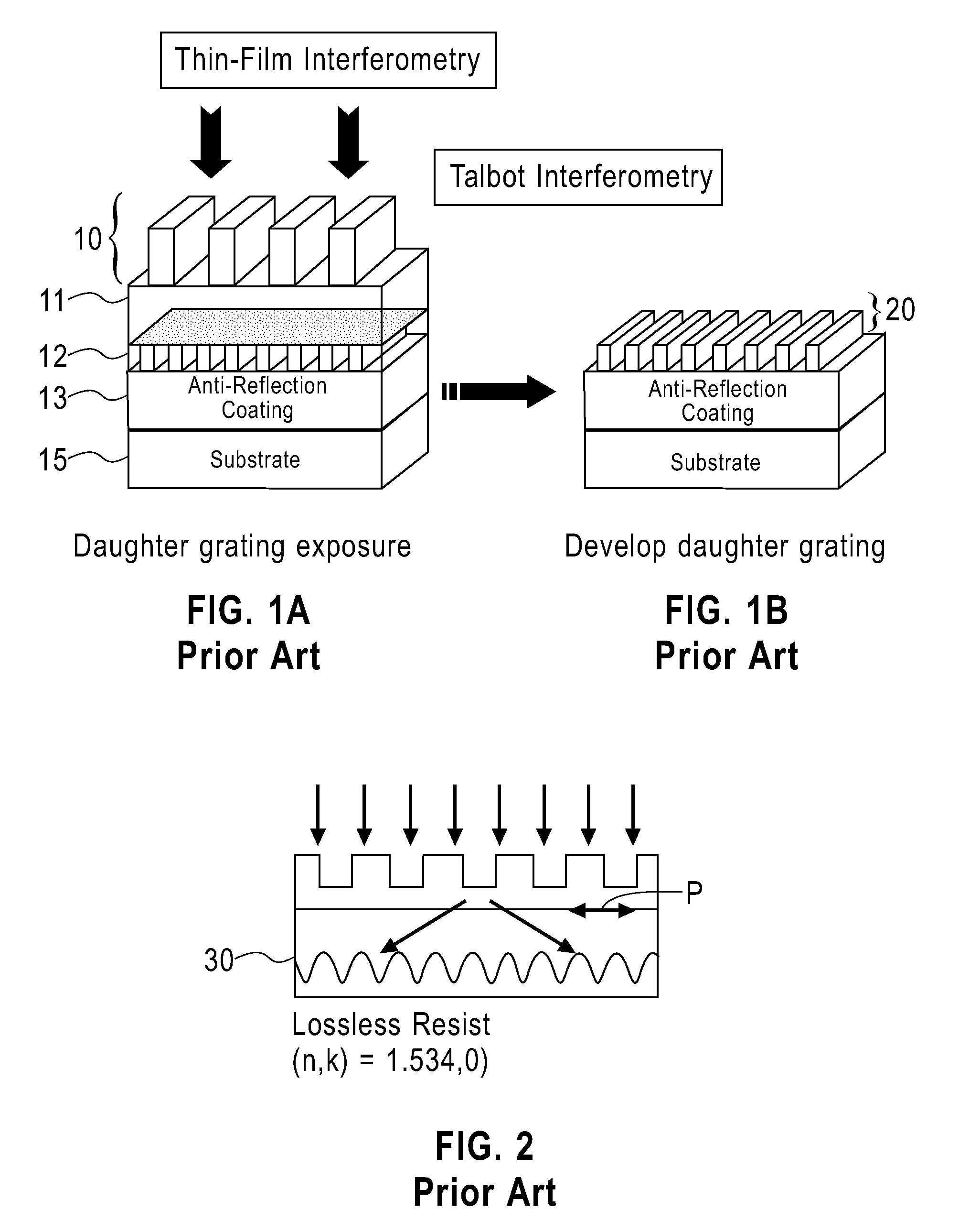
One drawback to Talbot lithography is that the printed features are restricted to periodic line / space patterns.
While there is a significant subset of
semiconductor devices whose design layouts are relatively simple (and moreover such devices may be of particular importance at the ultra-high resolutions where difficulties in device scaling make large and complex circuit layouts more problematic), pure line / space patterns are only of limited utility.
A second difficulty arises in fabricating the parent
grating.
Some of the state-of-the-art techniques described above can provide such fine resolutions, which can then be reduced further through Talbot lithography; however such spatial frequencies for the parent
grating fall near the limit of current lithographic technology, and can prove difficult to manufacture.
A more fundamental difficulty is that future
semiconductor technologies will require printing pitches that are considerably smaller than the wavelength, and under such circumstances electromagnetic effects due to interaction of the incident light with the
resist topography produces an undesired increase of the energy diffracted into the 0th order, hence critically degrading the double-frequency Talbot image in this regime.
For this reason a standard
grating structure will generally be unable to provide the sub-wavelength frequency-doubled
fringe pattern that is needed to achieve a resolution superior to current projection technology.
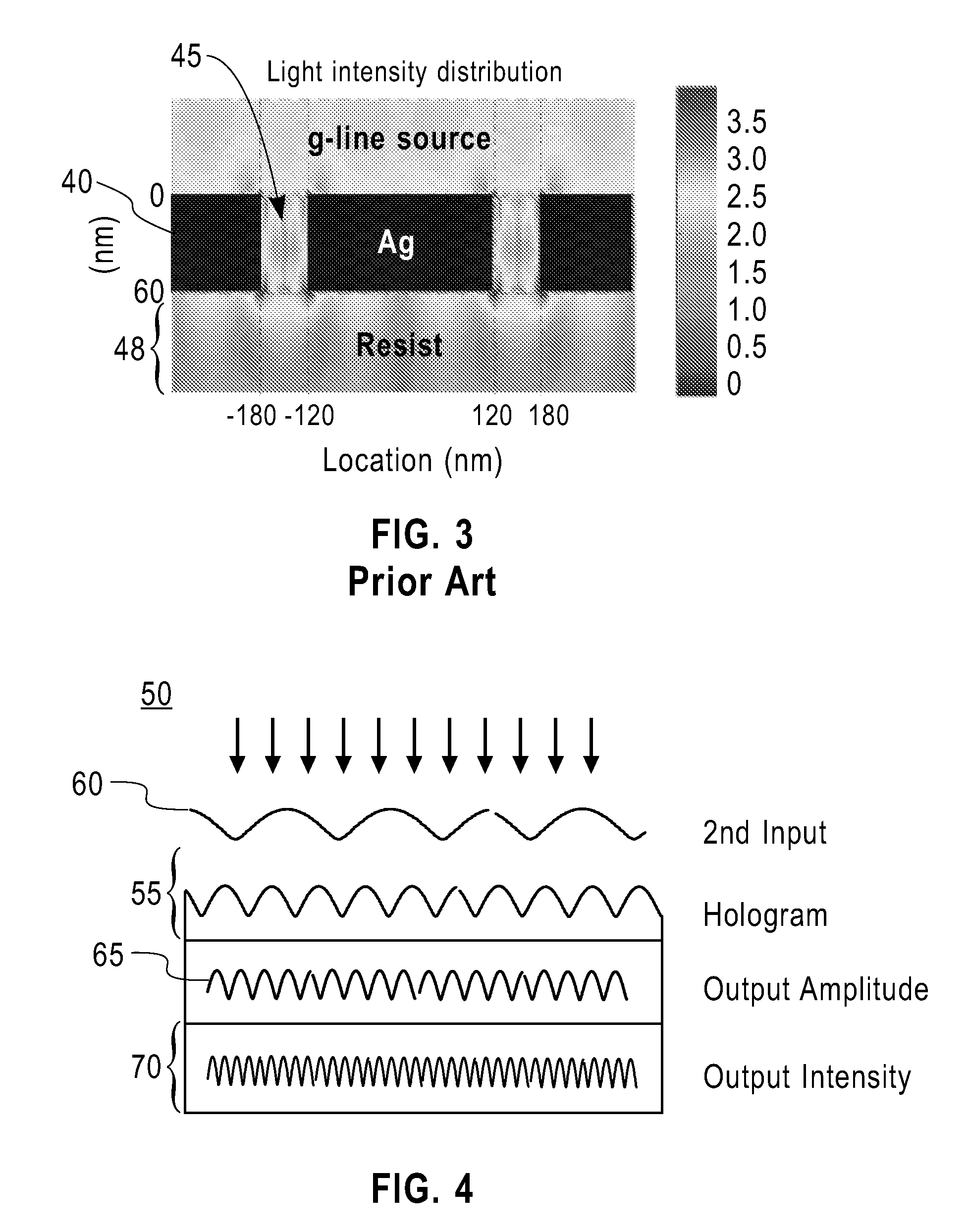
In this technique, complex electromagnetic effects also arise when light is transmitted through grating arrays (1D or 2D) of pinholes or slits in metallic films, particularly metals whose
dielectric constant has a large negative real part.
Thus far only gratings have been proposed for plasmonic lithography, limiting this technique to very specialized applications.
And, as with Talbot parent gratings for sub-wavelength spatial frequencies, analysis of the plasmonic gratings is numerically intensive.
A significant problem with the
solid immersion approach however, is that large-NA projection systems can only be optically corrected to the
diffraction limit over fields that are quite small; typically somewhat smaller than a
single chip, and far smaller than a
silicon wafer.
Solid immersion lithography is relatively impractical, and can only be expected to extend the spatial frequency limit of projection systems by a small margin since the refractive index of the final lens element that is contacted to the
resist stack is currently limited to n=1.56 or below.
Talbot lithography is relatively inflexible in the patterns it can produce, and it cannot easily provide
high contrast frequency doubling as feature sizes become strongly sub-wavelength, due to EMF enhancement of the zero order at these dimensions.
However, such a lens element (alternately referred to as a diffractive or holographic element) is not suitable as a final contacted lens surface in a lithographic
system that seeks to overcome the limitations imposed by the refractive index of the exit space by placing the final element in close proximity to the wafer.
In a conventional configuration, the holographic element can be spaced away from the
image field and given a larger
diameter, but this is not possible in a
solid immersion
system where materials limitations force the
high index space between the hologram and image to be quite thin.
A related problem is that the aberrations in a
Fresnel lens of such high power would be impossible to correct in a telecentric system.
The drawback to such a holographic approach is that the problem of fabricating an ultra-high-resolution image is simply re-posed as that of fabricating the hologram.
For this reason, the conventional holograms do not offer the desired path to improved resolution, since the resolution needed to fabricate them is in general no coarser than the resolution attainable in the diffracted patterns that they can form.

