Resin composition, insulating sheet with base, prepreg, multilayer printed wiring board and semiconductor device

Inactive Publication Date: 2010-03-18
SUMITOMO BAKELITE CO LTD
View PDF9 Cites 10 Cited by
  • Summary
  • Abstract
  • Description
  • Claims
  • Application Information

AI Technical Summary

Benefits of technology

[0024]The resin composition of the present invention is used for forming an insulating layer of a multilayer printed wiring board, wherein a surface roughness parameter Rvk value of the insulating layer is from 0.1 μm to 0.8 μm, measured after the insulating layer being formed with the resin composition, and subjected to roughening treatment.
[0025]By

Problems solved by technology

In such a semi-additive process, it is not preferable if concavity and convexity of a surface (degree of surface roughness) of the insulating layer are too large after the roughening treatment, since delay in speed of electric current passing a surface of copper, and decrease of hygroscopic solder heat resistance (solder heat resistance after app

Method used


Image

  • Resin composition, insulating sheet with base, prepreg, multilayer printed wiring board and semiconductor device
  • Resin composition, insulating sheet with base, prepreg, multilayer printed wiring board and semiconductor device

Examples


example 1

(1) Preparation of Resin Varnish

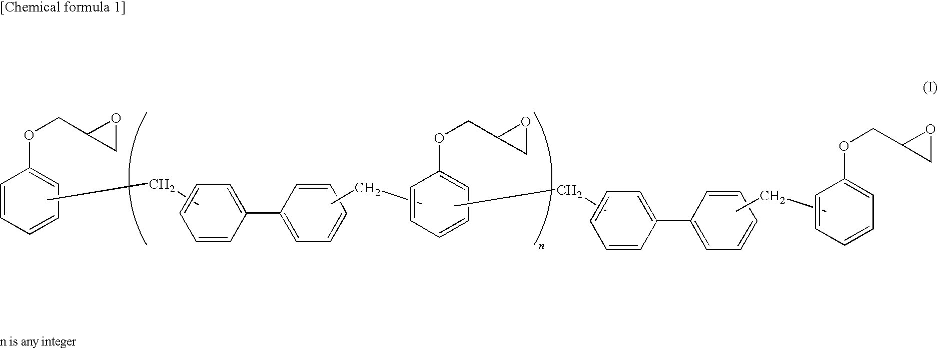
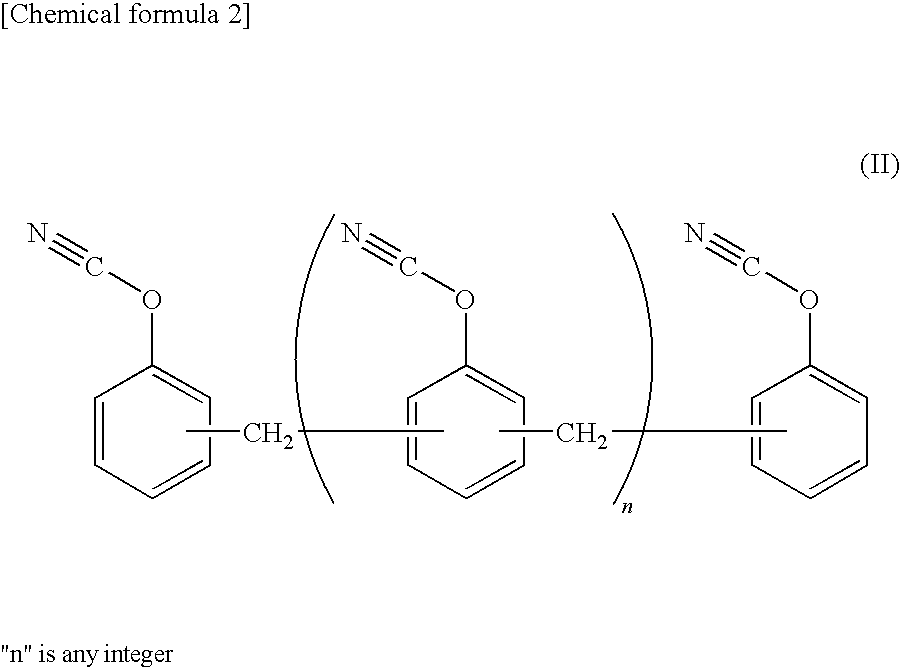
[0150]20 parts by weight of epoxy resin, 15 parts by weight of phenoxy resin A, 25 parts by weight of cyanate resin, and 0.05 parts by weight of curing catalyst were dissolved and dispersed in methyl ethyl ketone. Further, 40 parts by weight of inorganic filler A and 0.2 parts by weight of coupling agent A were added therein, and agitated for 10 minutes by means of a high speed agitator. Thus, a resin varnish having a solid content of 50 weight % was prepared.

(2) Production of Insulating Sheet on a Base

[0151]The resin varnish obtained above was applied on one side of PET (polyethylene terephthalate) film having a thickness of 25 μm by means of a comma coater so as to form an insulation film having a thickness of 60 μm after drying. Then, the pet film was dried for 10 minutes at 160° C. by means of a drying machine. Thus, an insulating sheet provided on a base was produced.

(3) Production of Multilayer Printed Wiring Board 1

[0152]The insulating sheet on...

example 2

[0158]15 parts by weight of epoxy resin, 20 parts by weight of phenoxy resin B, 25 parts by weight of cyanate resin and 0.05 parts by weight of curing catalyst were dissolved and dispersed in methyl ethyl ketone. Further, 40 parts by weight of inorganic filler A and 0.2 parts by weight of coupling agent B were added therein, and agitated for 10 minutes by means of a high speed agitator. Thus, a resin varnish having a solid content of 50 weight % was prepared.

[0159]Using the resin varnish, an insulating sheet on a base and multilayer printed wiring boards 1 and 2 were obtained in the same manner as Example 1. The surface roughness Rvk after the roughening treatment was 0.25 μm.

example 3

[0160]20 parts by weight of epoxy resin, 20 parts by weight of phenoxy resin A, 35 parts by weight of cyanate resin and 0.05 parts by weight of curing catalyst were dissolved and dispersed in methyl ethyl ketone. Further, 25 parts by weight of inorganic filler A and 0.2 parts by weight of coupling agent C were added therein and agitated for 10 minutes by means of a high speed agitator. Thus, a resin varnish having a solid content of 50 weight % was prepared.

[0161]Using the resin varnish, an insulating sheet on a base and multilayer printed wiring boards 1 and 2 were obtained in the same manner as Example 1. The surface roughness Rvk after the roughening treatment was 0.35 μm.


PUM

PropertyMeasurementUnit
Percent by massaaaaaaaaaa
Particle sizeaaaaaaaaaa

Abstract

The present invention provides a resin composition which can produce a multilayer printed wiring board not causing peeling and crack in a thermal shock test such as a cooling/heating cycle, and having high heat resistance and low-thermal expansion characteristics, when the resin composition is used for an insulating layer of the multilayer printed wiring board; and also an insulating sheet provided on a base, a prepreg, a multilayer printed wiring board and a semiconductor device using thereof. The resin composition is used for forming an insulating layer of the multilayer printed wiring board, wherein a surface roughness parameter Rvk value of the insulating layer is from 0.1 μm to 0.8 μm, measured after the insulating layer being formed with the resin composition, and subject to roughening treatment.

Description

TECHNICAL FIELD [0001]The present invention relates to a resin composition, an insulating sheet provided on abase, a prepreg, a multilayer printed wiring board and a semiconductor device.BACKGROUND ART [0002]In recent years, with growing demand of higher function of electronics, high-density integration within electronic components and high-density mounting of electronic components have been developed. Printed wiring boards capable of high-density mounting and so on used for the electronic components have been developed in miniaturization and high density than ever before. In order to increase the density in the printed wiring boards, buildup multilayer printed wiring boards have been widely employed (for example, see Japanese Patent Application Laid-open (JP-A) No. H07-106767).[0003]Buildup multilayer printed wiring boards are generally produced by laminating insulating layers and conducting circuit layers, the insulating layer having a thickness of 100 μm or less and being constit...

Claims


Application Information

Patent Timeline
IPC IPC(8): H05K1/00B32B27/38C08K3/36C08L101/10C08G67/00
CPCB32B15/08B32B27/36C08K5/5425C08K5/548C08L63/00Y10T428/24917H05K3/4626H05K2201/0209Y10T428/254Y10T428/252Y10T428/287H05K3/389B32B5/022B32B5/024B32B15/14B32B15/20B32B27/16B32B27/18B32B27/20B32B27/26B32B27/28B32B27/38B32B2260/021B32B2260/046B32B2262/02B32B2262/0261B32B2262/0269B32B2262/0276B32B2262/0284B32B2262/10B32B2262/101B32B2264/102B32B2307/206B32B2307/306B32B2307/3065B32B2307/308B32B2307/50B32B2307/538B32B2307/72B32B2307/7265B32B2457/00B32B2457/08Y10T428/249994Y10T428/31511Y10T428/24994Y10T428/31663C08K7/18C08J5/24C08J5/18H01L23/14C08K3/013C08K3/36C08J2363/00
Inventor KIMURA, MICHIO
Owner SUMITOMO BAKELITE CO LTD
Why Eureka
Try Eureka