Pll circuit

Inactive Publication Date: 2010-04-22
RENESAS TECH CORP +1
View PDF3 Cites 49 Cited by
  • Summary
  • Abstract
  • Description
  • Claims
  • Application Information

AI Technical Summary

Benefits of technology

[0016]Accordingly, an object of the present invention is to provide a technique capable of s

Problems solved by technology

More particularly, in microfabrication, device variations and increases of consumption curre

Method used


Image

  • Pll circuit
  • Pll circuit
  • Pll circuit

Examples


first embodiment

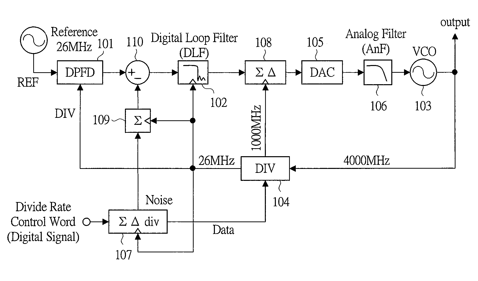
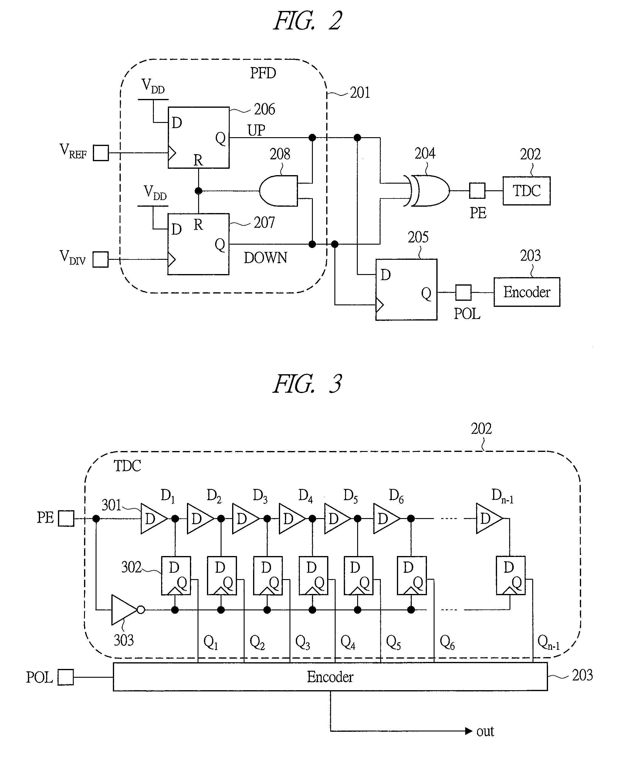
[0042]FIG. 1 is a block diagram showing a configuration example of a PLL (Phase-Locked Loop) according to a first embodiment of the present invention; FIG. 2 is a circuit diagram showing a configuration example of a digital phase frequency detector (DPFD) 101 in the PLL circuit according to the first embodiment; FIG. 3 is a circuit diagram showing a configuration example of a phase difference digital converter (TDC) 202 included in the DPFD; FIG. 4 is a circuit diagram showing a configuration example of a Sigma-Delta modulator (ΣΔdiv) 107; and FIG. 5 is a circuit diagram showing a configuration example of an analog filter (AnF) 106.

[0043]First, the example of the configuration of the PLL circuit according to the first embodiment will be described with reference to FIG. 1. The PLL circuit of the first embodiment is, for example, a semiconductor integrated circuit, which is formed on one semiconductor chip by a known semiconductor manufacturing technology.

[0044]The PLL circuit of FIG....

second embodiment

[0060]FIG. 7 is a block diagram showing a configuration example of a PLL (Phase-Locked Loop) circuit according to a second embodiment of the present invention.

[0061]As compared with the first embodiment, the PLL circuit according to the second embodiment has a same noise-elimination type of the fractional-N type but has a different configuration after the DLF 102. In the second embodiment, an oscillator (DCO & VCO) 701 is controlled by using upper bit side of the output of the DLF 102. A DCO (Digital Controlled Oscillator) part in the oscillator 701 performs coarse adjustment of frequency by digital control, and a VCO (Voltage Controlled Oscillator) part in the oscillator 701 performs fine adjustment of frequency by analog control. More particularly, upper bit (can be 1 bit or multiple bits) of the output of the DLF 102 is inputted to a digital control terminal of the oscillator 701 and lower bit (can be 1 bit or multiple bits) of the DLF 102 is inputted to the Sigma Delta modulator...

third embodiment

[0064]In a third embodiment, an application example of the PLL circuits of the first and second embodiments described above will be described.

[0065]FIG. 9 is a block diagram showing a configuration of a transceiving RF-IC for the pan-European digital cellular system GSM (BRIGHT).

[0066]The BRIGHT in FIG. 9 adopts a direct conversion system for data reception and an off-set PLL system for data transmission. A local oscillator and a frequency synthesizer 901 may adopt the PLL circuits of the first and second embodiments described above.

[0067]FIG. 10 is a block diagram showing a configuration of a transceiving RF-IC for the pan-European digital cellular system EDGE (BRIGHT).

[0068]The BRIGHT in FIG. 10 adopts a direct conversion system for data reception and a polar loop system for data transmission. A local oscillator and a frequency synthesizer 1001 may adopt the PLL circuits of the first and second embodiments described above.

[0069]FIG. 11 is a block diagram showing a configuration of...


PUM


Abstract

A technique for suppressing quantization noise generated due to digitizing an analog circuit in a PLL circuit is provided. The PLL circuit comprises: a digital phase frequency detector which detects (compares) phases and frequencies of a reference signal and a frequency-divided signal and converts the same to a digital value; a digital loop filter which eliminates high-frequency noise components from an output of the digital phase frequency comparator; a digital-analog converter which converts a digital value of an output of the digital loop filter to an analog value; an analog filter which eliminates a high-frequency noise component from an output of the digital-analog converter; a voltage controlled oscillator whose frequency is controlled based on an output of the analog filter; and a frequency divider which divides the frequency of the voltage controlled oscillator and outputs the frequency-divided signal.

Description

TECHNICAL FIELD OF THE INVENTION[0001]The present invention relates to a PLL (Phase Locked Loop) circuit. More particularly, the present invention relates to a technique for suppressing noise to be problematic in digitizing PLL circuits.BACKGROUND OF THE INVENTION[0002]RF-IC used in cell phones and wireless LAN still has high potential for development. Currently, development of RF-IC has been progressed to 1-chip integration with a BB-IC (Baseband IC). Accordingly, it has been required to develop RF-IC in a sub-micron CMOS process used for BB-IC. Since RF-ICs are often analog circuits, current and area of an RF-IC tend to be increased when using the sub-micron CMOS process where device deviations are increased. More particularly, in microfabrication, device variations and increases of consumption current and area in an analog circuit due to an increase of gate capacitance will be problematic. Replacing the analog circuit with a digital circuit is one possible countermeasure.[0003]Th...

Claims


Application Information

Patent Timeline
IPC IPC(8): H03L7/08
CPCH03L7/089H03L7/093H03L2207/06H03L7/1976H03L7/099
Inventor UEDA, KEISUKEUOZUMI, TOSHIYAYAMAMOTO, SATORUSAMATA, MITSUNORIMOHN, RUSSELL P.DEC, ALEKSANDERSUYAMA, KEN
Owner RENESAS TECH CORP
Why Eureka
Try Eureka