Compound magnetic nanowires for tco replacement

a technology of compound magnetic nanowires and conductive films, which is applied in the direction of conductive layers on insulating supports, non-metal conductors, magnetic bodies, etc., can solve the problems that the combination of electrical conductivity and optical transparency available from thin films comprising nanowires has not been fully optimized, and achieves good optical transparency, good optical transparency, and low electrical sheet resistance

Inactive Publication Date: 2010-04-29
APPLIED MATERIALS INC
View PDF22 Cites 17 Cited by
  • Summary
  • Abstract
  • Description
  • Claims
  • Application Information

AI Technical Summary

Benefits of technology

[0006]Embodiments of this invention provide an optically transparent conductive layer with a desirable combination of low electrical sheet resistance and good optical transparency. The transparent conductive layer is comprised of magnetic nanowires and / or magnetic nanoparticles which are (1) at a low enough density to provide good optical transparency, and (2) arranged to optimize electrical conductivity. The properties of the transparent conductive layer may be optimized to provide good optical transmission, greater than 90% over the wavelength range of 250 nm to 1.1 microns, and low sheet resistance, less than 20 Ohm / square at room temperature. The concepts and methods of this invention allow for integration of the transparent conductive layer into devices such as solar cells, displays and light emitting diodes.

Problems solved by technology

Clearly, the combination of electrical conductivity and optical transparency that is available from thin films comprising nanowires has yet to be fully optimized.

Method used


Image

  • Compound magnetic nanowires for tco replacement
  • Compound magnetic nanowires for tco replacement
  • Compound magnetic nanowires for tco replacement

Examples


Embodiment Construction

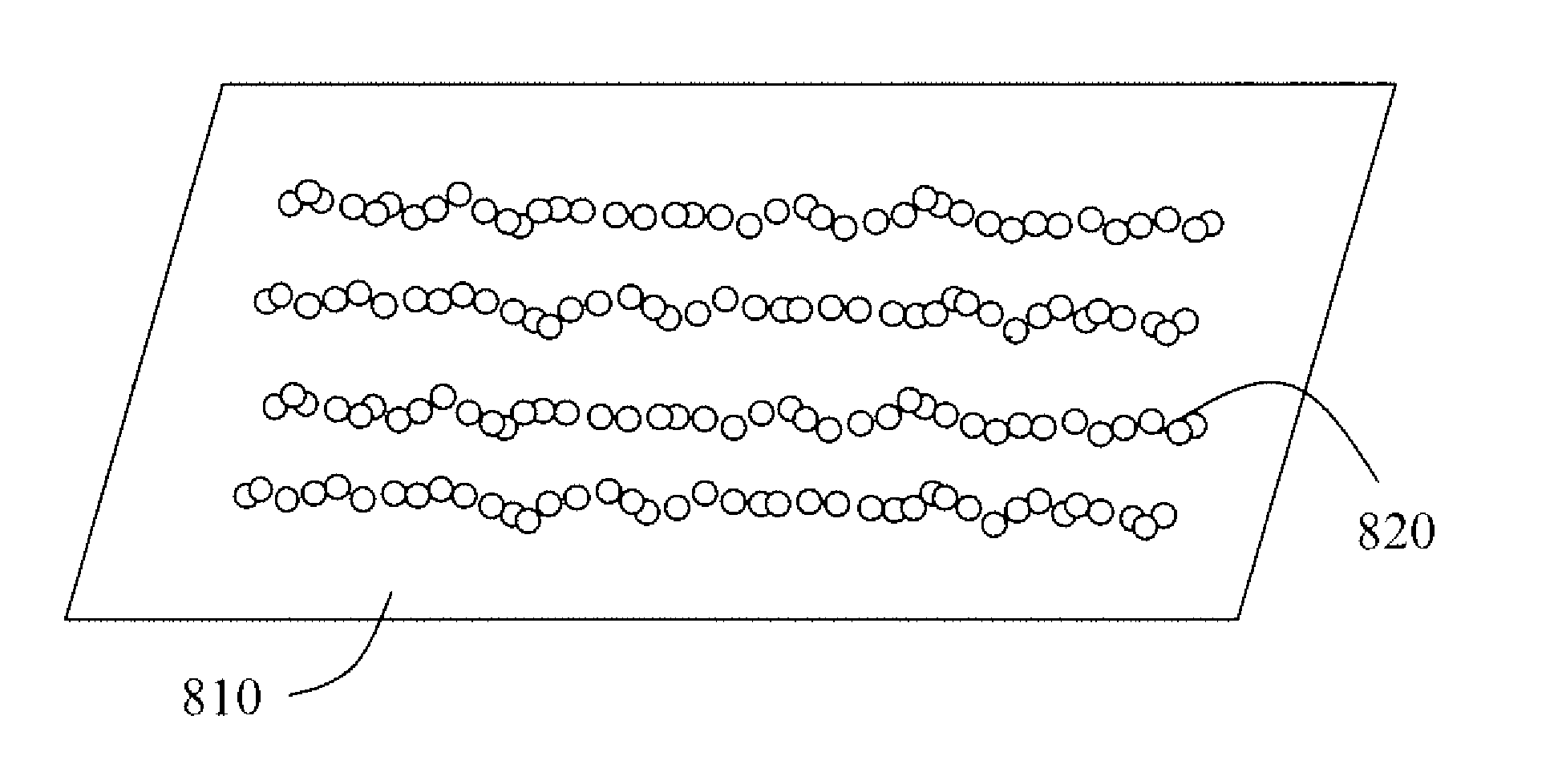
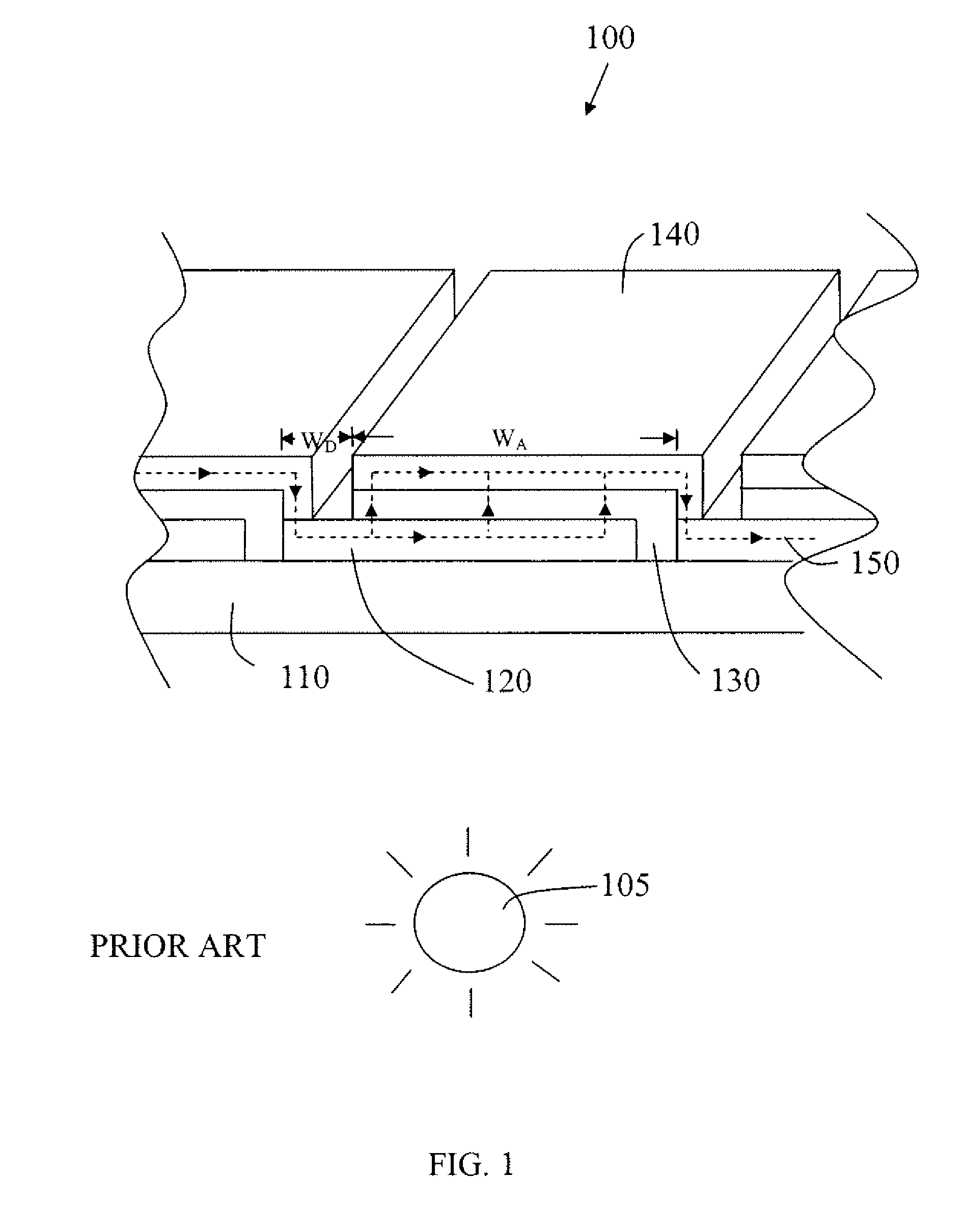
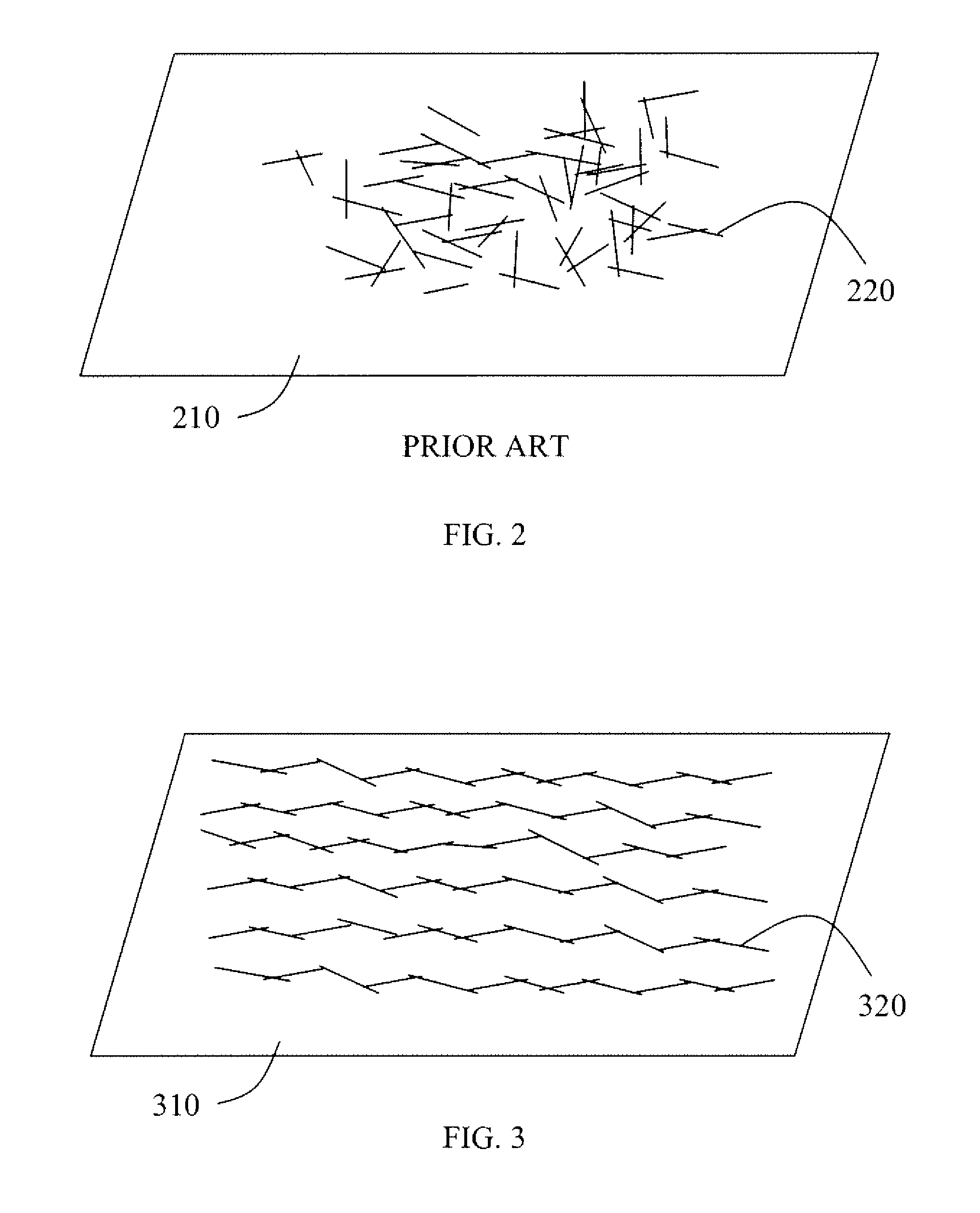
[0023]The present invention will now be described in detail with reference to the drawings, which are provided as illustrative examples of the invention so as to enable those skilled in the art to practice the invention. Notably, the figures and examples below are not meant to limit the scope of the present invention to a single embodiment, but other embodiments are possible by way of interchange of some or all of the described or illustrated elements. Moreover, where certain elements of the present invention can be partially or fully implemented using known components, only those portions of such known components that are necessary for an understanding of the present invention will be described, and detailed descriptions of other portions of such known components will be omitted so as not to obscure the invention. In the present specification, an embodiment showing a singular component should not be considered limiting; rather, the invention is intended to encompass other embodimen...


PUM

PropertyMeasurementUnit
Magnetic fieldaaaaaaaaaa
Densityaaaaaaaaaa
Electrical conductoraaaaaaaaaa

Abstract

This invention provides an optically transparent electrically conductive layer with a desirable combination of low electrical sheet resistance and good optical transparency. The conductive layer comprises a multiplicity of compound magnetic nanowires in a plane, the compound nanowires being aligned roughly (1) parallel to each other and (2) with the long axes of the compound nanowires in the plane of the layer, the compound nanowires further being configured to provide a plurality of continuous conductive pathways, and wherein the density of the multiplicity of compound magnetic nanowires allows for substantial optical transparency of the conductive layer. A compound magnetic nanowire may comprise a silver nanowire covered by a layer of magnetic metal such as nickel or cobalt. Furthermore, a compound magnetic nanowire may comprise a carbon nanotubes (CNT) attached to a magnetic metal nanowire. A method of forming the conductive layer on a substrate includes: depositing a multiplicity of compound magnetic conductive nanowires on the substrate and applying a magnetic field to form the compound nanowires into a plurality of conductive pathways parallel to the surface of the substrate.

Description

CROSS-REFERENCE TO RELATED APPLICATIONS[0001]This application is a Continuation in Part of U.S. application Ser. No. 12 / 419,178, filed Apr. 6, 2009, which is a Continuation in Part of U.S. application Ser. No. 12 / 258,263, filed Oct. 24, 2008.FIELD OF THE INVENTION[0002]The present invention relates generally to transparent conductive films and more specifically to a transparent conductive film comprising compound magnetic nanowires.BACKGROUND OF THE INVENTION[0003]Optically transparent conductor layers are used in a variety of applications where a transparent conductor is either required or provides an advantage. Applications using transparent conductors include: liquid crystal displays, plasma displays, organic light emitting diodes, solar cells, etc. The transparent conducting oxides (TCOs), such as indium tin oxide and zinc oxide, are the most commonly used transparent conductor materials. However, TCO films represent a compromise between electrical conductivity and optical trans...

Claims


Application Information

Patent Timeline
IPC IPC(8): H01B5/00B05B5/12
CPCB82Y25/00H01B1/02H01B1/04H01B1/08H01F1/0081Y10T29/49206H01J2217/49207H01L51/5206H01F1/445H01F1/0054H01J9/02H01B5/14H01B1/00B82B3/00B82B1/00H10K50/81
Inventor VERHAVERBEKE, STEVENNALAMASU, OMKARAMPUSHPARAJ, VICTOR L.GOUK, ROMAN
Owner APPLIED MATERIALS INC
Why Eureka
Try Eureka