Conductive oxynitride and method for manufacturing conductive oxynitride film

a technology of oxynitride and conductive oxynitride, which is applied in the direction of non-metal conductors, conductors, metal/alloy conductors, etc., can solve the problems of significant unevenness of light-transmitting conductive films which have been crystallized by heat treatment, deformation of the conductive film, and inability to meet the requirements of the application, etc., to achieve the effect of suppressing crystallization

Active Publication Date: 2010-05-06
SEMICON ENERGY LAB CO LTD
View PDF7 Cites 45 Cited by
  • Summary
  • Abstract
  • Description
  • Claims
  • Application Information

AI Technical Summary

Benefits of technology

[0007]The method for depositing an indium oxide-tin oxide alloy (ITO) film in an atmosphere to which hydrogen or water vapor are added is effective for suppressing crystallization during the film deposition. However, even an indium oxide-tin oxide alloy (ITO) film deposited by this method is crystallized by heat treatment at high temperatures after the deposition. Specifically, in the case where an indium oxide-tin oxide alloy (ITO) film is heated at temperatures over 200° C. to 250° C., crystallization proceeds.

Problems solved by technology

However, even an indium oxide-tin oxide alloy (ITO) film deposited by this method is crystallized by heat treatment at high temperatures after the deposition.
A light-transmitting conductive film which has been crystallized by heat treatment has significant unevenness on a surface thereof.
In the case where the light-transmitting conductive film having the significantly uneven surface is used for an electrode of a thin film element, a short circuit is likely to occur and thus reliability of the element is degraded.
Further, since the light-transmitting conductive film which has been crystallized by heat treatment is not easily dissolved in an etchant, it is also a problem that microfabrication is required to be completed before heat treatment and thus the order of steps is restricted.

Method used


Image

  • Conductive oxynitride and method for manufacturing conductive oxynitride film
  • Conductive oxynitride and method for manufacturing conductive oxynitride film
  • Conductive oxynitride and method for manufacturing conductive oxynitride film

Examples


embodiment 1

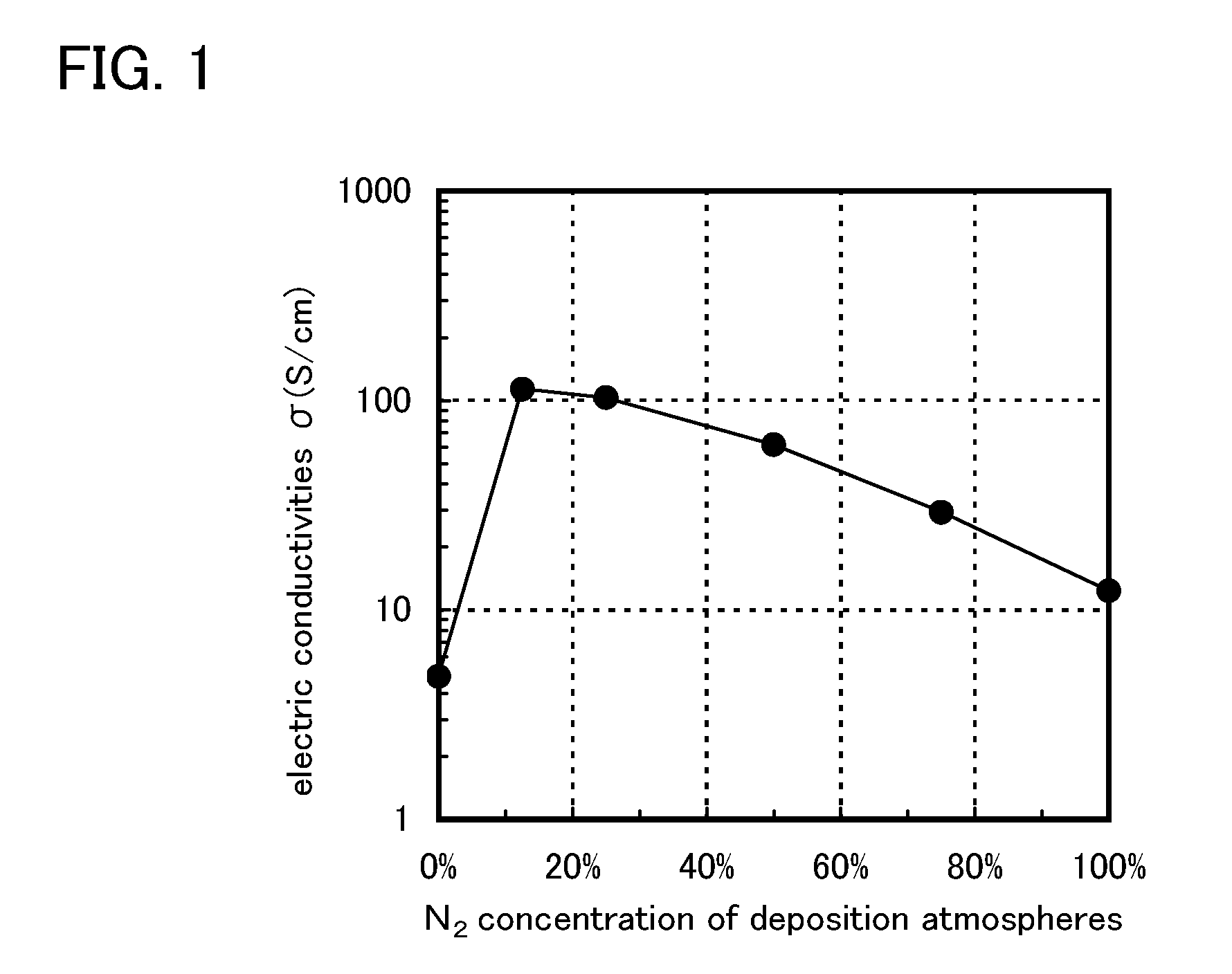
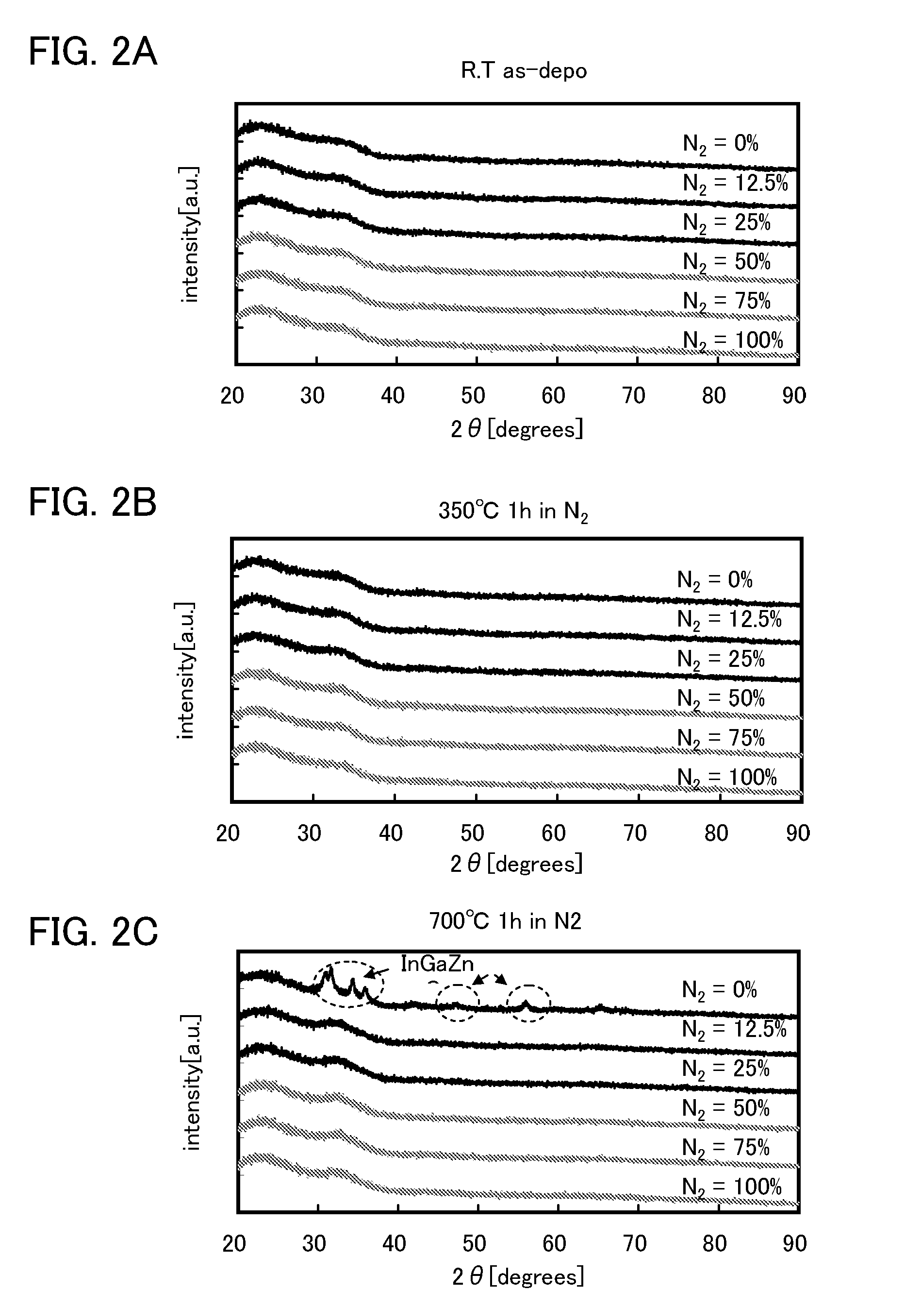
[0051]This embodiment will describe a light-transmitting conductive oxynitride film which is an embodiment of the present invention and a manufacturing method thereof. Specifically, described will be a method for manufacturing a light-transmitting conductive oxynitride film, in which an oxynitride film containing indium, gallium, and zinc is deposited in an atmosphere containing a nitrogen gas, a compound serving as a supply source of hydrogen atoms is made to adsorb onto a surface of the oxynitride film, and then heat treatment is performed.

[0052]A substrate over which a conductive oxynitride is deposited is not particularly limited as long as it can withstand a process temperature of this manufacturing process.

[0053]For example, a non-alkali glass substrate manufactured by a fusion method or a float method, such as a substrate of barium borosilicate glass, aluminoborosilicate glass, or aluminosilicate glass, a ceramic substrate, a plastic substrate, or the like can be used. Furthe...

embodiment 2

[0067]This embodiment will describe a light-transmitting conductive oxynitride film which is an embodiment of the present invention and a manufacturing method thereof. Specifically, described will be a method for manufacturing a conductive oxynitride film, in which an oxynitride film containing indium, gallium, and zinc is deposited in an atmosphere containing a nitrogen gas, and then heat treatment is performed on the oxynitride film in an atmosphere containing a compound serving as a supply source of hydrogen atoms.

[0068]The oxynitride film containing indium, gallium, and zinc is deposited over a substrate in a manner similar to that of Embodiment 1.

[0069]Next, the substrate over which the oxynitride film containing indium, gallium, and zinc is deposited is carried out of a deposition chamber to a furnace for heat treatment without being exposed to the air. Specifically, a multi-chamber apparatus where the deposition chamber is connected to a heat treatment chamber with a load loc...

embodiment 3

[0075]This embodiment will describe a light-transmitting conductive oxynitride film which is an embodiment of the present invention and a manufacturing method thereof. Specifically, described will be a method for manufacturing a conductive oxynitride film, in which an oxynitride film containing hydrogen, indium, gallium, and zinc is deposited in an atmosphere containing nitrogen and a compound serving as a supply source of hydrogen atoms, and then heat treatment is performed.

[0076]A substrate similar to that of Embodiment 1 is used. The oxynitride film containing indium, gallium, and zinc into which hydrogen is diffused is deposited in an atmosphere containing hydrogen and nitrogen.

[0077]Specifically, the deposition is performed by a sputtering method in an atmosphere containing a hydrogen gas and a nitrogen gas so that the composition ratios of nitrogen (N) to oxygen (O) (N / O) in the oxynitride film containing indium, gallium, and zinc range from 5 atomic % to 80 atomic %, preferab...


PUM

PropertyMeasurementUnit
temperaturesaaaaaaaaaa
strain pointaaaaaaaaaa
temperatureaaaaaaaaaa

Abstract

An electrode formed using a transparent conductive oxide is likely to be crystallized by heat treatment performed in the manufacturing process of a semiconductor device. In the case of a thin film element using an electrode having a significantly uneven surface due to crystallization, a short circuit is likely to occur and thus reliability of the element is degraded. An object is to provide a light-transmitting conductive oxynitride which is not crystallized even if subjected to heat treatment and a manufacturing method thereof. It is found that an oxynitride containing indium, gallium, and zinc, to which hydrogen atoms are added as impurities, is a light-transmitting conductive film which is not crystallized even if heated at 350° C. and the object is achieved.

Description

BACKGROUND OF THE INVENTION[0001]1. Field of the Invention[0002]The present invention relates to a conductive oxynitride and a manufacturing method thereof. In particular, the present invention relates to a conductive oxynitride formed using an oxynitride containing indium, gallium, and zinc and a method for manufacturing a conductive oxynitride film.[0003]2. Description of the Related Art[0004]In recent years, flat panel displays (such as liquid crystal display devices, light-emitting display devices, and electrophoretic display devices) have been actively developed. Most of them have a structure in which display or display light is seen through an electrode using a transparent conductive oxide. As a typical example of the transparent conductive oxide, an indium oxide-tin oxide (In2O3—SnO2) alloy (abbreviated to ITO) film formed using a target obtained by adding tin oxide to indium oxide and performing sintering can be given.[0005]A sputtering method has been widely employed as a m...

Claims


Application Information

Patent Timeline
Patent Type & Authority Applications(United States)
IPC IPC(8): H01L29/78H01B1/06B05D5/12C23C14/34
CPCC23C14/0057C23C14/0676C23C14/5846H01L27/1225H01L29/7869C04B35/58C04B2235/3284C04B2235/3286H01L27/124
Inventor SAKATA, JUNICHIROMARUYAMA, TETSUNORIIMOTO, YUKIASANO, YUJIKOEZUKA, JUNICHI
Owner SEMICON ENERGY LAB CO LTD
Why Eureka
Try Eureka