
OLED device with fluoranthene electron injection materials

Active Publication Date: 2010-05-13
GLOBAL OLED TECH
View PDF100 Cites 24 Cited by
  • Summary
  • Abstract
  • Description
  • Claims
  • Application Information

AI Technical Summary

Benefits of technology

[0021]Devices of the invention provide improvement

Problems solved by technology

While organic electroluminescent (EL) devices have been known for over two decades, their performance limitations have represented a barrier to many desirable applications.
However, these devices do not necessarily have all desired EL characteristics in terms of high luminance in combination with low drive voltages.

Method used


Image

  • OLED device with fluoranthene electron injection materials
  • OLED device with fluoranthene electron injection materials
  • OLED device with fluoranthene electron injection materials

Examples


example 1

Synthesis of Inventive Compound Inv-1

[0331]Inv-1 was synthesized as outlined in Scheme 1 and described below.

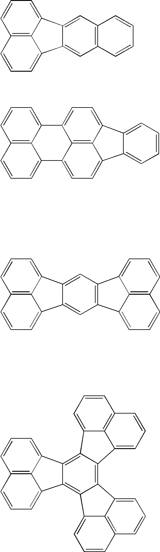
Preparation of 7,9-Diphenyl-8H-Cyclopent[a]acenaphthylen-8-one (1)

[0332]7,9-Diphenyl-8H-Cyclopent[a]acenaphthylen-8-one, (Acecyclone), (1) was prepared according to the procedure of W. Dilthey, I. ter Horst and W. Schommer; Journal fuer Praktische Chemie (Leipzig), 143, (1935), 189-210.

Preparation of 8-pyrid-3′-yl-7,10-diphenylfluoranthene (Inv-1)

[0333]Acecyclone (5.6 g, 16.0 mMol) and 2-ethynylpyridine (2.16 g, 21 mMol) were heated in 1,2-dichlorobenzene (50 mL) at 200° C. for 3 hours. After this period, the solution was cooled and added directly to a column of silica gel. Using pressure chromatography and eluting initially with heptane, 1,2-dichlorobenzene was removed. A gradient of ethyl acetate / heptane up to 50% ethyl acetate was then used to obtain a solution of product. After removal of most of the solvent (heptane / ethyl acetate) by evaporation, the product began to cry...

example 2

Electrochemical Redox Potentials and Estimated Energy Levels

[0334]LUMO and HOMO values are typically estimated experimentally by electrochemical methods. The following method illustrates a useful way to measure redox properties. A Model CHI660 electrochemical analyzer (CH Instruments, Inc., Austin, Tex.) was employed to carry out the electrochemical measurements. Cyclic voltammetry (CV) and Osteryoung square-wave voltammetry (SWV) were used to characterize the redox properties of the compounds of interest. A glassy carbon (GC) disk electrode (A=0.071 cm2) was used as working electrode. The GC electrode was polished with 0.05 μm alumina slurry, followed by sonication cleaning in Milli-Q deionized water twice and rinsed with acetone in between water cleaning. The electrode was finally cleaned and activated by electrochemical treatment prior to use. A platinum wire served as counter electrode and a saturated calomel electrode (SCE) was used as a quasi-reference electrode to complete a ...

example 3

Preparation of Blue-Light Emitting OLED Devices 3.1 through 3.6

[0339]A series of OLED devices (3.1 through 3.6) were constructed in the following manner:

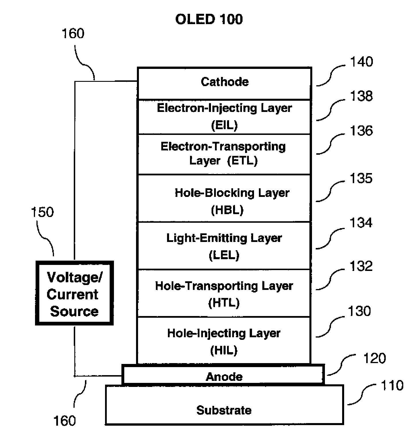
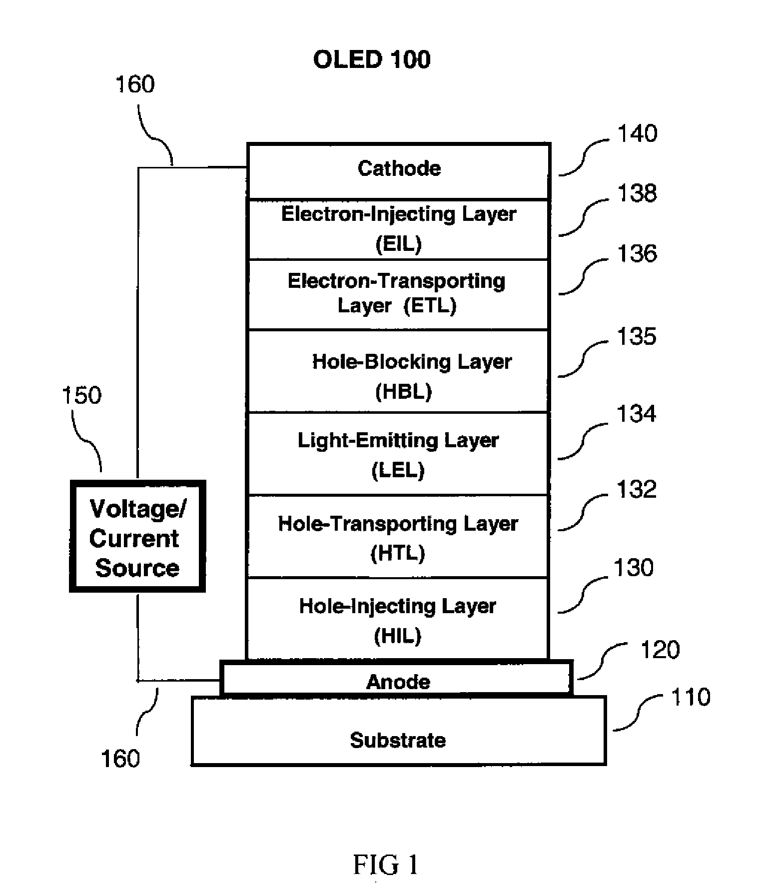
[0340]1. A glass substrate coated with an 85 nm layer of indium-tin oxide (ITO), as the anode, was sequentially ultrasonicated in a commercial detergent, rinsed in deionized water and exposed to oxygen plasma for about 1 min.

[0341]2. Over the ITO was deposited a 1 nm fluorocarbon (CFx) hole-injecting layer (HIL) by plasma-assisted deposition of CHF3 as described in U.S. Pat. No. 6,208,075.

[0342]3. Next a layer of hole-transporting material 4,4′-Bis[N-(1-naphthyl)-N-phenylamino]biphenyl (NPB) was deposited to a thickness of 95 nm.

[0343]4. A 20 nm light-emitting layer (LEL) corresponding to the host material P-4 and 1.5% by volume of FD-54 was then deposited.

[0344]5. An electron-transporting layer (ETL) consisting of a mixture of isomeric compounds FA-2 and FA-3 (60 / 40 ratio) at a thickness as shown in Table 2, was vacuum-deposited ov...


PUM

PropertyMeasurementUnit
Thicknessaaaaaaaaaa
Energyaaaaaaaaaa
Electric potential / voltageaaaaaaaaaa

Abstract

The invention provides an OLED device including a cathode, an anode, and having there between a light-emitting layer, further including, between the cathode and the light emitting layer, a first layer containing a fluoranthene compound including one and only one fluoranthene nucleus and having no aromatic rings annulated to the fluoranthene nucleus, the fluoranthene nucleus having independently selected aromatic groups in the 7,10-positions and an azine group in the 8- or 9-position, provided that the azine group is not a phenanthroline group. The OLED device desirably includes a second layer containing an alkali metal or alkali metal compound, located between the cathode and the first layer. The OLED device can also include a polycyclic aromatic hydrocarbon compound in the first layer or in a third layer located between the first layer and the light-emitting layer. Devices of the invention provide improvement in features such as efficiency and drive voltage.

Description

CROSS-REFERENCE TO RELATED APPLICATION[0001]Reference is made to U.S. patent application Ser. No. 11 / 924,629 by Begley et al. entitled “OLED DEVICE WITH CERTAIN FLUORANTHENE LIGHT-EMITTING DOPANTS,” filed Oct. 26, 2007, U.S. patent application Ser. No. 11 / 924,626 by Begley et al. entitled “OLED DEVICE WITH CERTAIN FLUORANTHENE HOST,” filed Oct. 26, 2007, U.S. patent application Ser. No. 11 / 924,631 by Begley et al., entitled “OLED DEVICE WITH FLUORANTHENE ELECTRON TRANSPORT MATERIALS,” filed Oct. 26, 2007, and U.S. patent application Ser. No. 12 / 266,802 by Begley et al. entitled “ELECTROLUMINESCENT DEVICE CONTAINING A FLOURANTHENE COMPOUND,” filed on Nov. 7, 2008, the disclosures of which are incorporated herein by reference.FIELD OF THE INVENTION[0002]This invention relates to an organic light-emitting diode (OLED) electroluminescent (EL) device having a light-emitting layer and an electron-transporting or electron-injecting layer including a specific type of fluoranthene compound.B...

Claims


Application Information

Patent Timeline
IPC IPC(8): H01J1/63
CPCC09K11/06C09K2211/1029C09K2211/107C09K2211/185H01L51/0055H01L2251/5384H01L51/0058H01L51/0072H01L51/5092H05B33/14H05B33/20H01L51/0056H10K85/624H10K85/623H10K85/626H10K85/6572H10K50/171H10K2101/90
Inventor BEGLEY, WILLIAM J.ANDRIEVSKY, NATASHALIAO, LIANG-SHENG
Owner GLOBAL OLED TECH
Learn More