

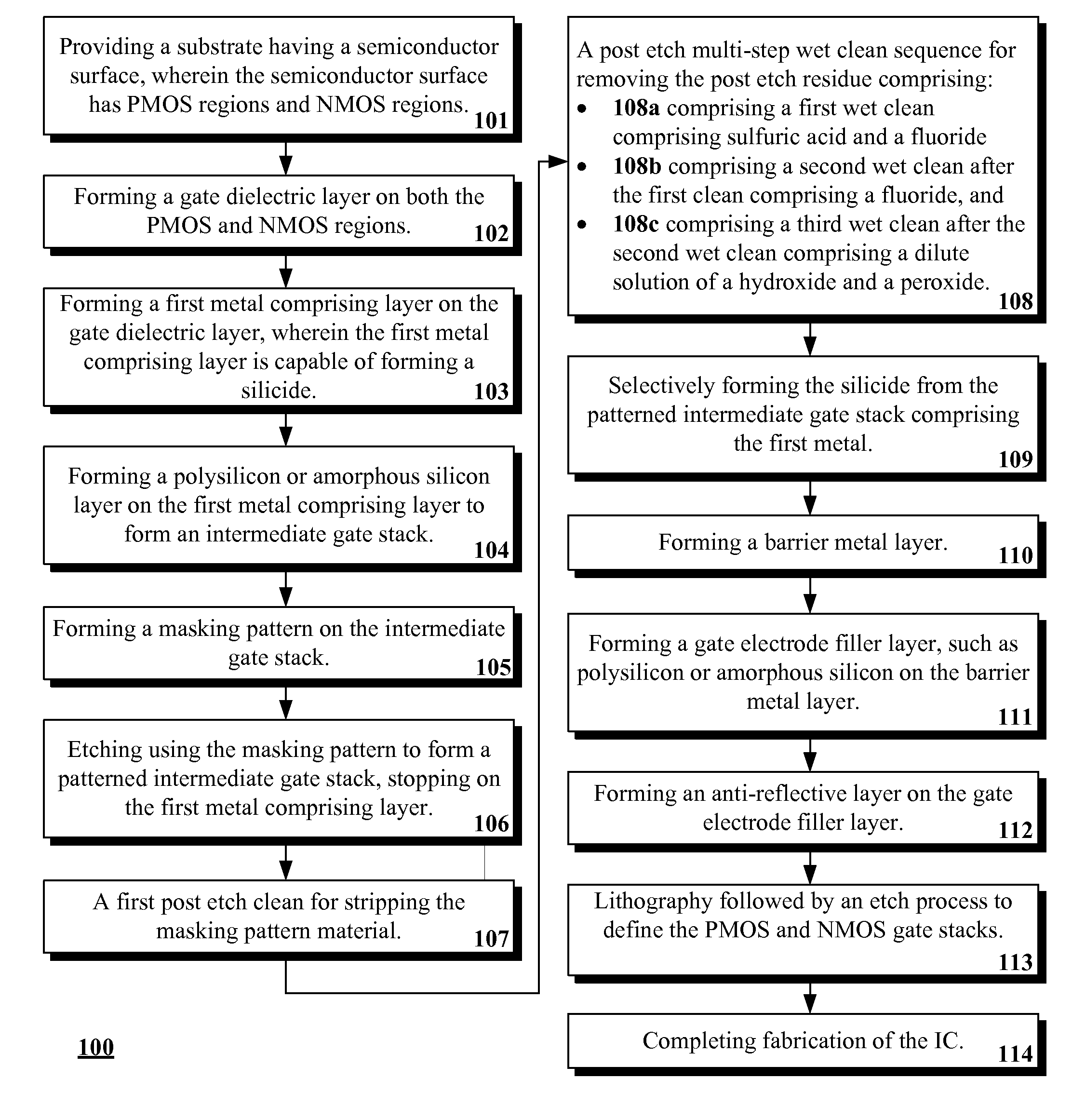
Post metal gate vt adjust etch clean
a technology of etch clean and metal gate, which is applied in the direction of basic electric elements, electrical equipment, semiconductor devices, etc., can solve the problems of generating residues that are impossible or at least difficult to remove, and achieve the effects of reducing residual particles, improving yield and reliability of such ics, and maintaining selectivity to exposed metals
- Summary
- Abstract
- Description
- Claims
- Application Information
AI Technical Summary
Benefits of technology
Problems solved by technology
Method used
Image

Examples
examples
[0024]The following non-limiting Examples serve to illustrate selected embodiments of the invention. It will be appreciated that variations in proportions and alternatives in elements of the components shown will be apparent to those skilled in the art and are within the scope of embodiments of the present invention.
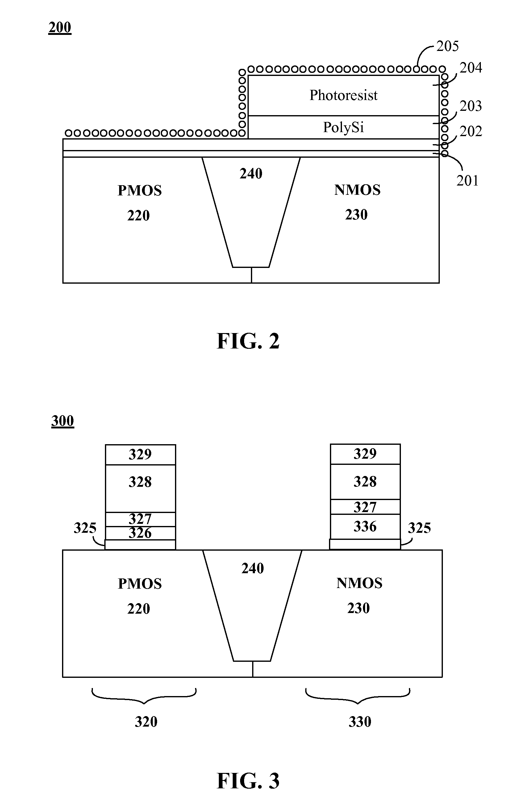
[0025]Wafers having the structure shown in FIG. 2 were prepared. The stack comprised a 2 nm thick layer of HfSiON gate dielectric 201, a W blanket first metal comprising layer 202 that was about 10 nm thick, a silicon layer 203 that was a 40 nm thick polysilicon layer and photoresist masking layer 204. Images were acquired and analyzed and particles counted using a KLA-2800 Stealth from KLA Instruments (KLA-Tencor Corporation, Milpitas, Calif. 95035)
[0026]In a first inventive embodiment, a hydrogen nitrogen reducing ash with a pressure 10 mtorr; power=1,500 Watts, 200 Watt back bias and 50 sccm N2 and 150 sccm H2 at 20° C. was used to remove the photoresist layer 204. Re...
PUM
| Property | Measurement | Unit |
|---|---|---|
| temperature | aaaaa | aaaaa |
| temperature | aaaaa | aaaaa |
| temperature | aaaaa | aaaaa |
Abstract
Description
Claims
Application Information