
Multiple band gapped cadmium telluride photovoltaic devices and process for making the same

a photovoltaic device and cadmium telluride technology, applied in the direction of sustainable manufacturing/processing, final product manufacturing, vacuum evaporation coating, etc., can solve the problems of limiting the short circuit current (jsub>sc/sub>) of the solar cell, low optical transmission coefficient of approximately 80%, and further complicated, etc., to achieve the effect of improving conversion efficiency

Active Publication Date: 2010-07-22
AUCMOS TECH USA INC
View PDF3 Cites 56 Cited by
  • Summary
  • Abstract
  • Description
  • Claims
  • Application Information

AI Technical Summary

Benefits of technology

[0018]The present invention addresses the drawback of the prior art CdTe photovoltaic device noted above and provides a CdTe photovoltaic device which absorbs photons from the red and near infrared part of the solar spectrum for improving conversion efficiency.
[0019]Accordingly, an object of the present invention is to provide a high efficiency CdTe photovoltaic device having multiple absorber layers designed for specific parts of the solar spectrum.

Problems solved by technology

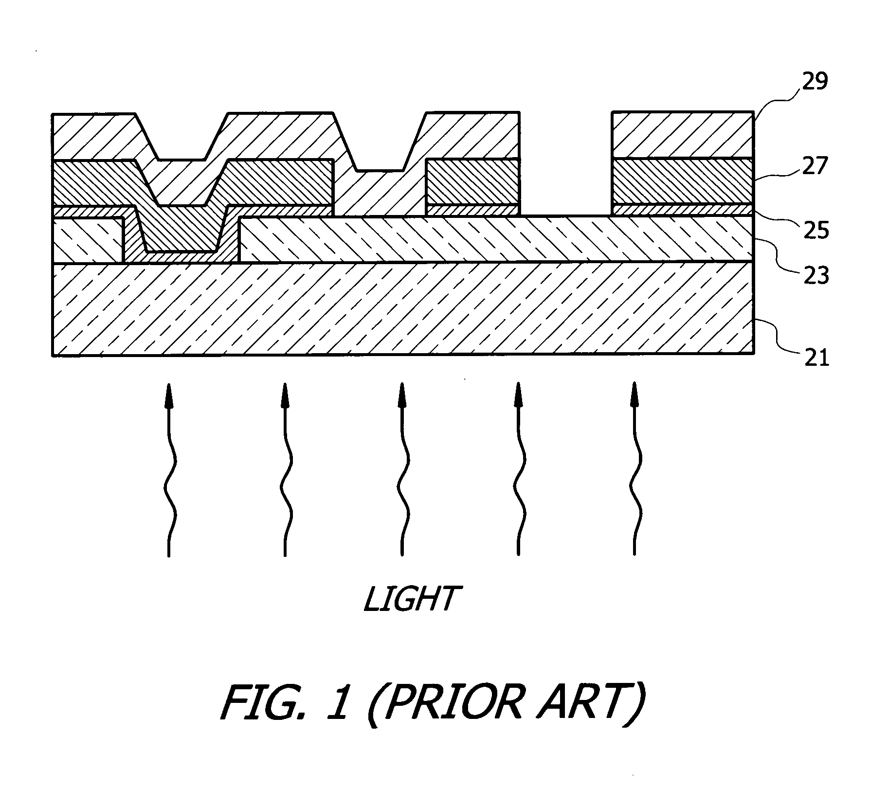
However, SnO2:F has a relatively low optical transmission coefficient of approximately 80%, which limits the short circuit current (Jsc) of the solar cell.
The thinning of the CdS window layer 25, however, may lead to pin-hole formation, which may cause a shunt between the front contact 23 and the CdTe absorber layer 27.
This is further complicated by the fact that some CdS is consumed during the subsequent CdTe deposition and post-deposition annealing described below.
There has been a trend to minimize the thickness of the CdTe absorber layer 27 in order to conserve the rare element tellurium (Te), because it is thought that there may not be adequate Te supply to fabricate enough CdTe photovoltaic devices to meet global demand.
If the work function of the contact does not exceed that of the p-type CdTe, a Schottky barrier would form at the interface which would hinder the carrier movement across the same, thereby decreasing the device efficiency.
Unlike crystalline silicon and copper indium gallium selenide (CIGS) photovoltaic devices which have lower band gap energies of about 1.1 eV to 1.2 eV and higher conversion efficiencies, CdTe photovoltaic device cannot effectively convert the red and near infrared part of the sunlight into electrical energy.

Method used


Image

  • Multiple band gapped cadmium telluride photovoltaic devices and process for making the same
  • Multiple band gapped cadmium telluride photovoltaic devices and process for making the same
  • Multiple band gapped cadmium telluride photovoltaic devices and process for making the same

Examples


Embodiment Construction

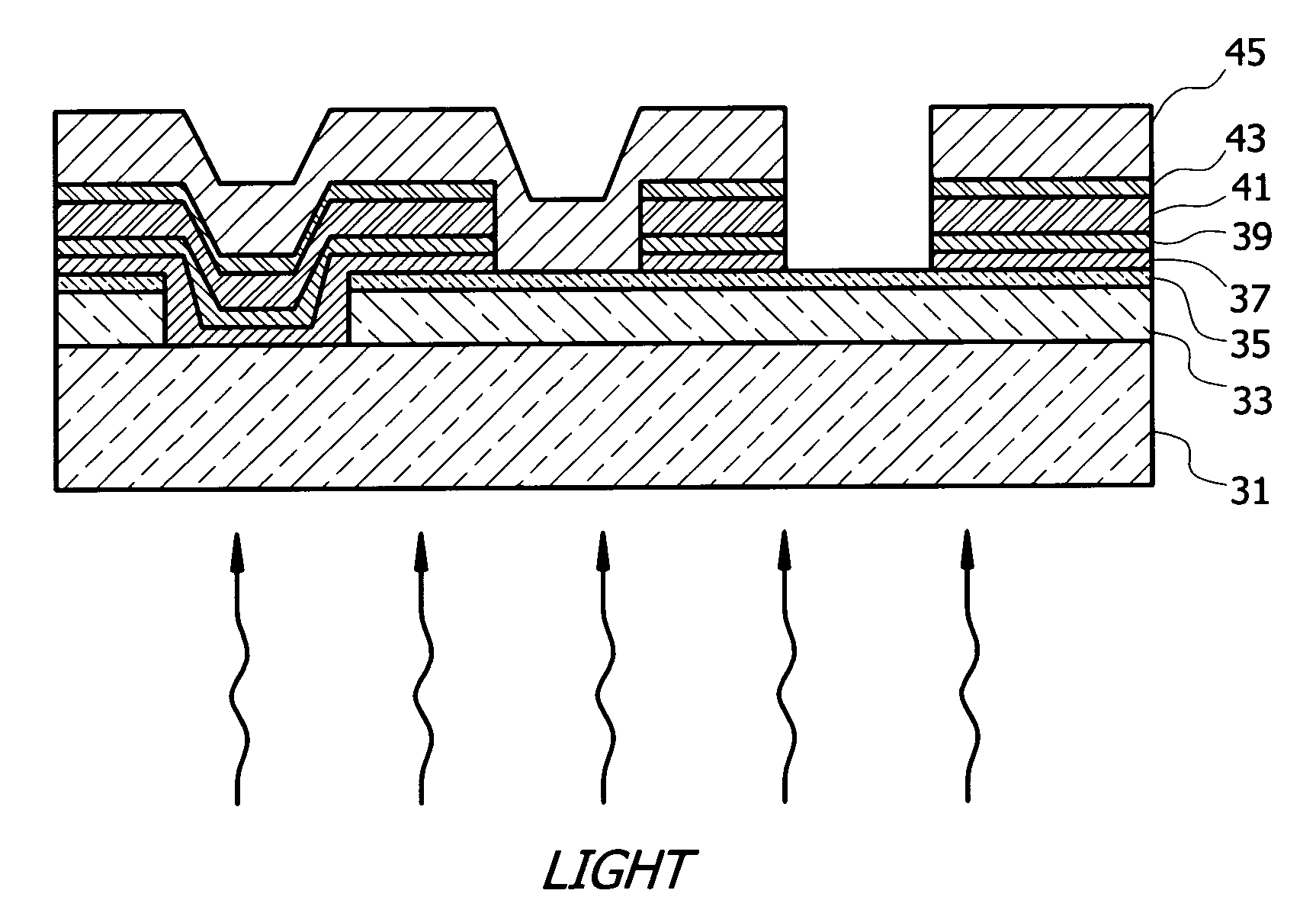
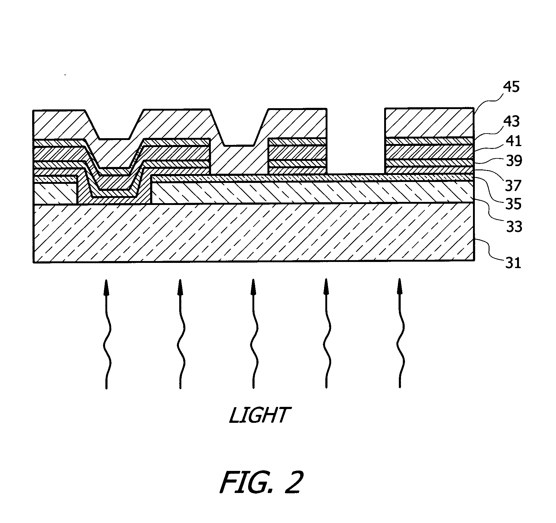
[0027]The present invention overcomes the inability of the conventional CdTe photovoltaic device to absorb low energy photons by the spectrum splitting or multi band gap approach, wherein multiple absorber layers with different band gap energies are employed to absorb photons from a wider range of the solar spectrum. Compared with the conventional CdTe absorber having a band gap energy of 1.45-1.5 eV, an absorber layer with a higher band gap energy can convert high energy photons to higher open circuit voltage (Voc), while an absorber with a lower band gap energy can absorb lower energy photons and allow more efficient use of the solar spectrum.

[0028]The preferred embodiment of the present invention as applied to a CdTe photovoltaic device having three absorber layers will now be described with reference to FIG. 2. Referring now to FIG. 2, the illustrated device has an optically transparent dielectric substrate 31, through which radiant energy or sunlight enters the device; a layer ...


PUM

PropertyMeasurementUnit
Temperatureaaaaaaaaaa

Abstract

A heterojunction photovoltaic device for the production of electrical energy in response to the incident light includes an optically transparent substrate, a front contact formed of an transparent conductive oxide for collecting light generated charge carriers, an n-type window layer formed of cadmium sulfide or zinc sulfide, a p-type absorber structure disposed on the window layer, thereby forming a rectification junction therebetween, and a back contact comprising at least one metal layer. The p-type absorber structure has a plurality of p-type absorber layers in contiguous contact. Each absorber layer contains cadmium as a principal constituent and has a different composition and a different band gap energy. The first absorber layer is in contiguous contact with the n-type window layer. The band gap energy progressively decreases from the first absorber layer to the last absorber layer in the p-type absorber structure.

Description

RELATED APPLICATIONS[0001]The present application is a continuation-in-part application of U.S. provisional patent application, Ser. No. 61 / 205,560, filed Jan. 21, 2009, for HYBRID SPUTTERING AND VAPOR TRANSPORT DEPOSITION PROCESS FOR MULTIPLE BAND-GAPPED CADMIUM TELLURIDE PHOTOVOLTAIC DEVICES, by Yung-Tin Chen, included herein by reference and for which benefit of the priority date is hereby claimed.FIELD OF THE INVENTION[0002]The present invention relates to a cadmium telluride photovoltaic device having multiple absorber layers with different band gap energies to improve photo conversion efficiency.BACKGROUND OF THE INVENTION[0003]Photovoltaic technology offers great potential as an alternative source of electrical energy. Among various types of thin film solar cell technologies, cadmium telluride (CdTe) semiconductor based solar cells have emerged to be one of the leading candidates for large scale, low cost photovoltaic power. The band gap energy of CdTe (1.45-1.5 eV) is well s...

Claims


Application Information

Patent Timeline
IPC IPC(8): H01L31/00C23C14/34
CPCH01L31/02963H01L31/0725Y02E10/543H01L31/1836H01L31/073Y02P70/50
Inventor CHEN, YUNG-TIN
Owner AUCMOS TECH USA INC
Learn More