Semiconductor device provided with thin film transistor and method for manufacturing the semiconductor device

Inactive Publication Date: 2010-07-22
SHARP KK
View PDF5 Cites 29 Cited by
  • Summary
  • Abstract
  • Description
  • Claims
  • Application Information

AI Technical Summary

Benefits of technology

[0049]According to the present invention, the degree of crystallinity of the source/drain regions and the region to be a channel region can be increased and the element to be a donor or an acceptor that has been added to the source/drain regions can be activated more efficiently as well. As a result, the resistance in the source/drain regions can be reduced, and therefore, a thin-film transistor that has higher performance, and can operate at higher speeds, than conventional ones is provided.
[0050]In addition, according to the present invention, such a high-performance semiconductor device with a thin-film transistor can be fabricated without complicating the manufacturing process overly or increasing the manufacturing cost significantly.
[0051]According to the semiconductor device manufacturing process of the present invention, by introducing a rare-gas element to regions of a semiconductor film to be source/drain regions, the d

Problems solved by technology

A conventional TFT, however, has rather high source-drain resistance, which is one of the factors causing deterioration in its device performance.
Among these techniques, the furnace annealing process can be adopted if the substrate is a small glass motherboard but is difficult to apply to a situation where a glass substrate in as big a size as of more than 500 mm square is used.
This is because the furnace annealing process usually causes a lot of thermal damage that would make the substrate shrink under the heat.
However, the laser annealing system itself is too expensive and complicated to ensure good stability in the manufacturing process.
That is why considering the productivity and manufacturing cost, such an expensive and complicated system should not be used as a matter of principle unless it is absolutely necessary to use it to crystallize a semiconductor film, for example.
Ne

Method used


Image

  • Semiconductor device provided with thin film transistor and method for manufacturing the semiconductor device
  • Semiconductor device provided with thin film transistor and method for manufacturing the semiconductor device
  • Semiconductor device provided with thin film transistor and method for manufacturing the semiconductor device

Examples


Example

Embodiment 1

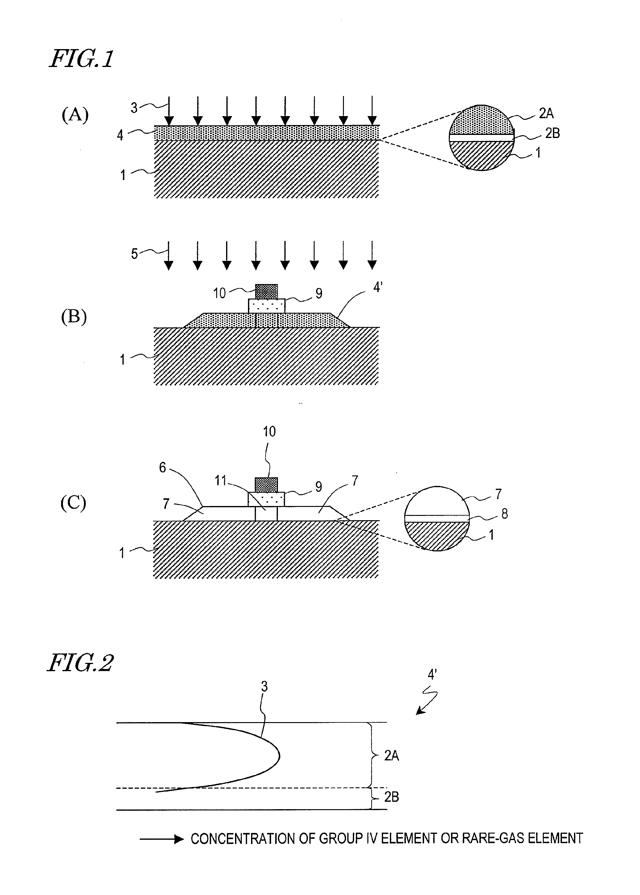
[0113]FIGS. 6(A) through 6(H) are schematic cross-sectional views illustrating respective manufacturing process steps to fabricate a thin-film transistor as a first specific preferred embodiment of the present invention. In the Following description of the first preferred embodiment, it will be described how to fabricate a p-channel TFT with a top gate structure on a glass substrate. The TFT of this preferred embodiment can be used not only as a pixel switching element or a driver circuit component for an active-matrix-addressed LCD or an organic EL display device but also as a component of a thin-film integrated circuit.

[0114]First of all, as shown in FIG. 6(A), an undercoat film 152 of silicon dioxide is deposited by plasma CVD process, for example, to a thickness of approximately 100-500 nm on a glass substrate 151, and then an intrinsic (i-type) amorphous silicon (a-Si) film 153 is deposited to a thickness of approximately 20-80 nm (e.g., 50 nm) thereon.

[0115]The und...

Example

Embodiment 2

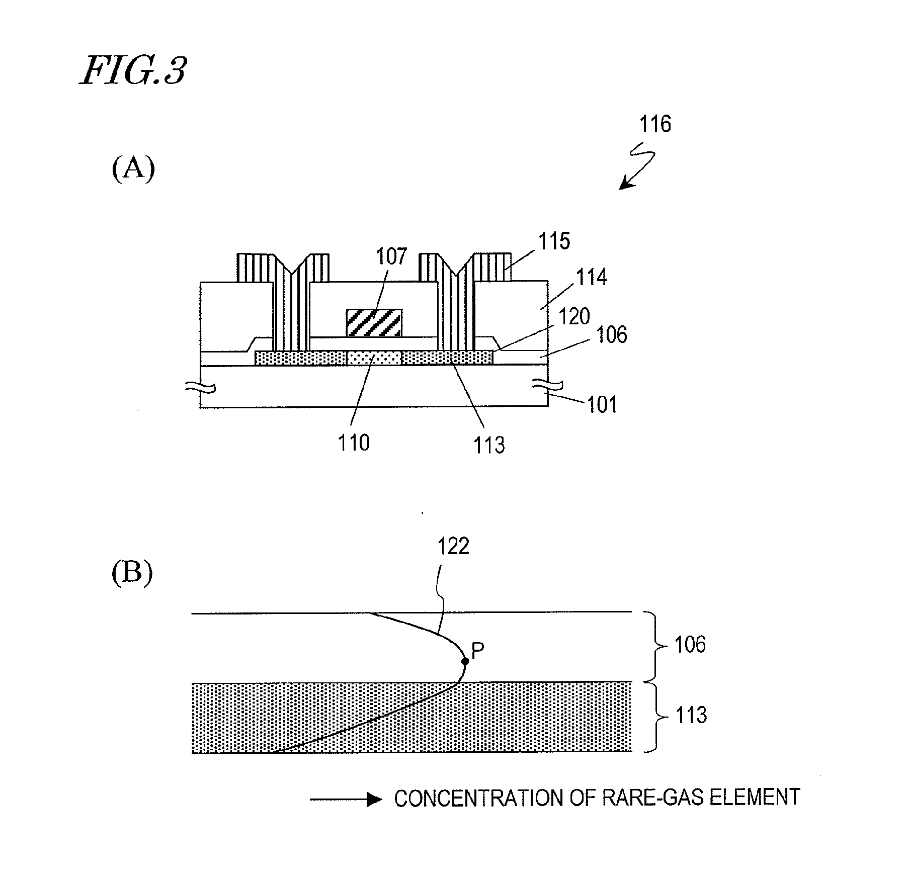
[0134]Hereinafter, a second specific preferred embodiment of the present invention will be described with reference to the accompanying drawings. In the following description of the second preferred embodiment, it will be described how to fabricate a circuit with a CMOS structure, in which an n-channel TFT and a p-channel TFT are arranged to operate complementarily with each other and which will be used as a peripheral driver circuit for an active-matrix-addressed LCD or an ordinary thin-film circuit, on a glass substrate.

[0135]FIGS. 8(A) through 8(G) are schematic cross-sectional views illustrating respective manufacturing process steps to fabricate an n-channel TFT and a p-channel TFT according to this preferred embodiment.

[0136]First of all, as shown in FIG. 8(A), first and second undercoat films 202 and 203 are deposited in this order on the surface of a substrate 201 to prevent impurities from diffusing from the glass substrate. And then a silicon film with an amorp...

Example

Embodiment 3

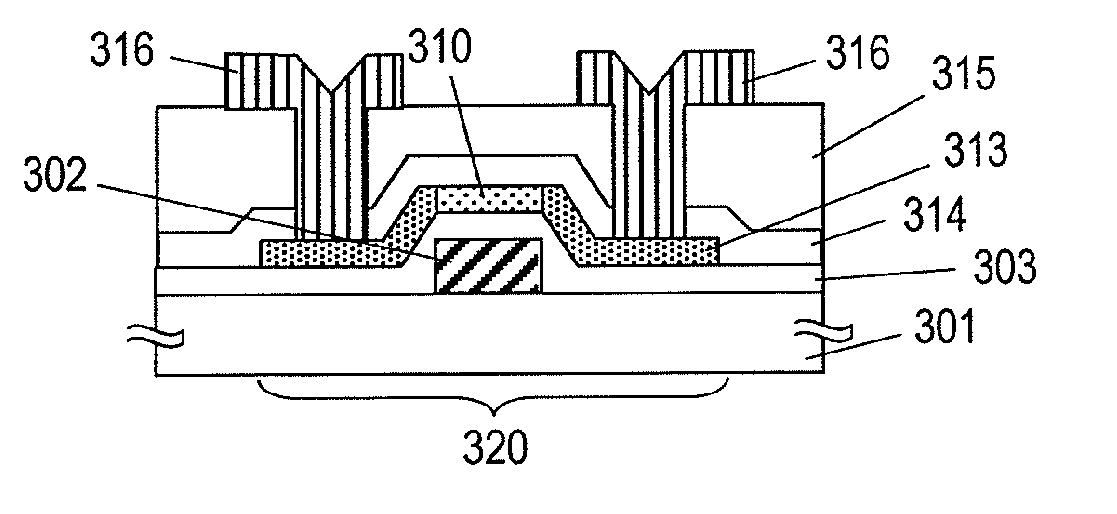
[0157]Hereinafter, a third preferred embodiment of the present invention will be described with reference to the accompanying drawings. In the preferred embodiments of the present invention described above, TFTs with a top gate structure are fabricated. On the other hand, the preferred embodiment to be described below is a method for fabricating a p-channel TFT with a bottom gate structure on a glass substrate. The TFT of this preferred embodiment can be used not only as a pixel switching element or a driver circuit component for an active-matrix-addressed LCD or an organic EL display device but also as a component of a thin-film integrated circuit.

[0158]FIGS. 10(A) through 10(H) are schematic cross-sectional views illustrating respective process steps to fabricate a p-channel TFT according to this preferred embodiment.

[0159]First, as shown in FIG. 10(A), a gate electrode 302 is formed on a glass substrate 301. Considering its thermal resistance that the metal film will ...


PUM


Abstract

A semiconductor device includes at least one thin-film transistor 116, which includes: a crystalline semiconductor layer 120 including a region 110 to be a channel region and source and drain regions 113; a gate electrode 107 for controlling the conductivity of the region 110 to be a channel region; a gate insulating film 106 arranged between the semiconductor layer 120 and the gate electrode 107; and source and drain electrodes 115 connected to the source and drain regions 113, respectively. At least one of the source and drain regions 113 contains an element to be a donor or an acceptor and a rare-gas element, but the region 110 to be a channel region does not contain the rare-gas element. The atomic weight of the rare-gas element is greater than that of the element to be a donor or an acceptor. The concentration of the rare-gas element in the at least one region as measured in the thickness direction thereof decreases continuously from the upper surface of the at least one region toward its lower surface.

Description

TECHNICAL FIELD[0001]The present invention relates to a semiconductor device including a thin-film transistor and a method for fabricating such a device.BACKGROUND ART[0002]A thin-film transistor (TFT) is used as a switching element to be provided for not only each pixel in the display area of an active-matrix-addressed LCD but also its driver circuit as well. In the driver circuit, in particular, a CMOS (complementary metal oxide semiconductor) circuit is usually formed by two TFTs of mutually different conductivity types. In those applications, the TFTs should have even better performance and operate at even higher response speeds.[0003]A conventional TFT, however, has rather high source-drain resistance, which is one of the factors causing deterioration in its device performance.[0004]The source / drain regions of a TFT are usually defined by implanting dopant ions into a semiconductor film by ion doping process and then performing a heat treatment process to activate the ions impl...

Claims


Application Information

Patent Timeline
IPC IPC(8): H01L33/00H01L29/786H01L21/336
CPCH01L27/1214H01L29/78618H01L29/66765H01L29/66757H01L27/127H01L27/1274
Inventor MAKITA, NAOKIHASHIMOTO, MASATO
Owner SHARP KK
Why Eureka
Try Eureka