Eureka AIR delivers breakthrough ideas for toughest innovation challenges, trusted by R&D personnel around the world.

Slit-scan multi-wavelength confocal lens module and slit-scan microscopic system and method using the same

a confocal lens module and multi-wavelength technology, applied in the field of three-dimensional optical surface profilometry, can solve the problems of significantly reduced wafer manufacturing yield, whole surface of inspected wafer, time-consuming, etc., and achieve the effect of optimizing the performance of the confocal lens modul

Active Publication Date: 2010-07-29
NAT TAIPEI UNIV OF TECH
View PDF16 Cites 68 Cited by
  • Summary
  • Abstract
  • Description
  • Claims
  • Application Information

AI Technical Summary

Benefits of technology

[0008]The object of the present invention is to provide a slit-scan multi-wavelength confocal lens module, which utilizes at least two lenses having chromatic aberration for splitting a broadband light field into a plurality of continuously linear spectral lights having different focal lengths respectively while projecting the plurality of continuously linear spectral lights onto an object. Unlike the conventional diffractive optical element having drawback of lower numerical aperture (NA) so that it can't be combined with the objective, the numerical aperture (Na) of the at least two lenses having chromatic aberration are about the same as those conventional objective lens such that they can be used directly as the objective lens Moreover, the problem relating to the field curvature is considered and calibrated during the designing of the at least two lenses having chromatic aberration in the confocal lens module so that performance of the confocal lens module is optimized as well as its size is minimized
[0009]Another object of the present invention is to provide a slit-scan multi-wavelength confocal lens module, being capable of not only enabling a broadband light field to be split into continuously linear spectral lights, but also enabling the broadband light field to be focused on a same plane after being reflected so as to overcome the problems relating to the field curvature and simplify the complex of conventional linear dispersion systems.
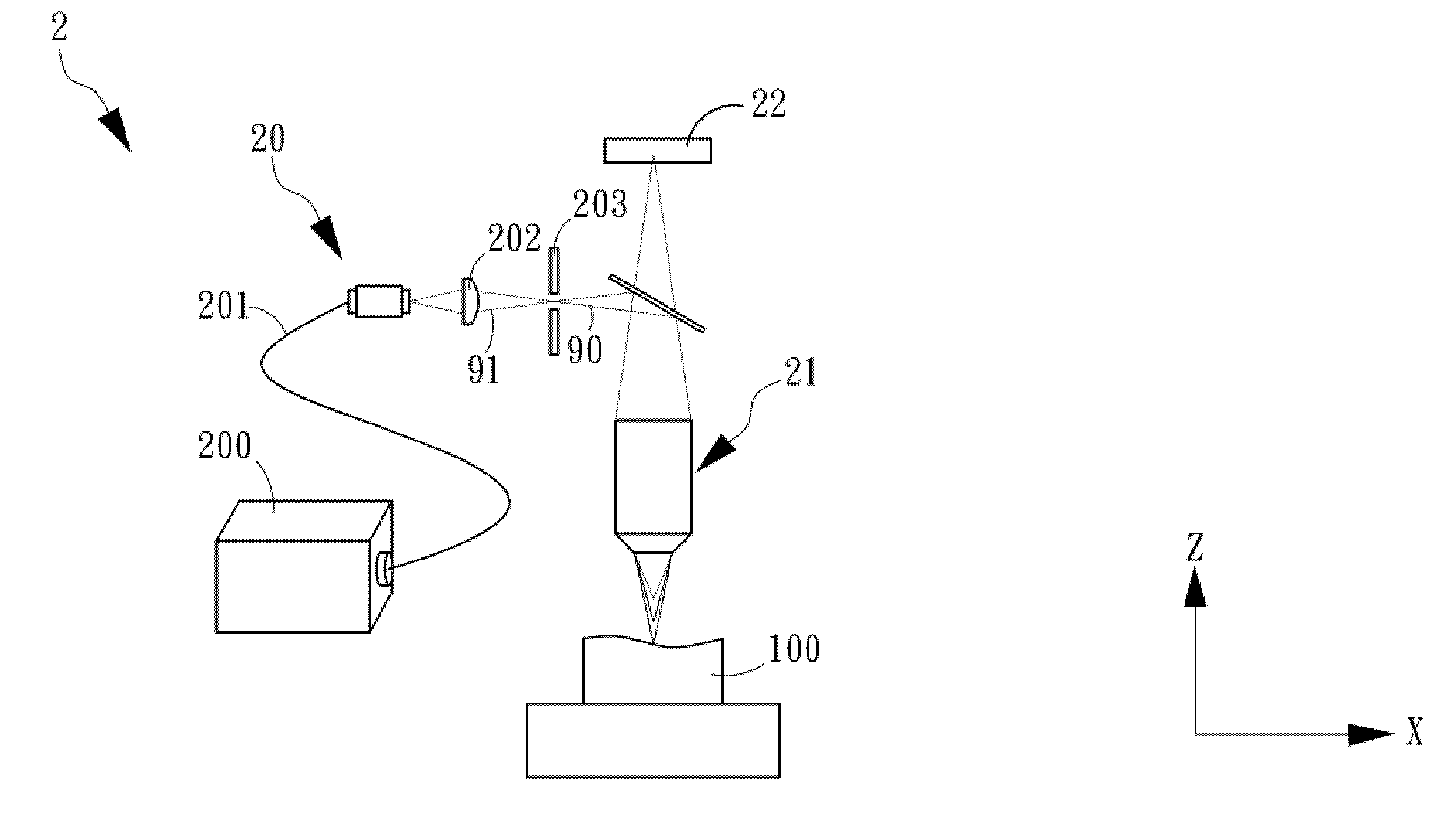
[0010]It is yet another object of the present invention to provide a slit-scan multi-wavelength confocal microscopic method and system, capable of using specific lens of chromatic aberration for modulating a broad band light field to produce the axial chromatic aberration light comprising a plurality of sub linear light fields having different focal lengths and then obtain the reflected light spectrum with respect to surface of an object. Following this, the spectrum is spatially filtered by a slit and then a peak position with respect to the filtered spectrum for every measuring point along the scanning line is detected by a spectrometer for generating the sectional profile of the measured surface efficiently and accurately, thereby, the measuring speed of the confocal microscopic method and system can be improved greatly so that they can be adapted to be used as an online measuring method and system.
[0011]It is further another object of the invention to provide a slit-scan multi-wavelength confocal microscopic method and system, being capable of obtaining a full-field surface profile of an object by a linear displacement movement, so as to overcome the shortcoming of point measurement of the conventional confocal microscopic method and system.
[0014]Yet, in another exemplary embodiment of the invention, a slit-scan multi-wavelength confocal microscopic method is provided, which comprises the steps of: providing a linear light field; using a chromatic dispersion objective lens for dispersing the linear light field thereby generating an axial chromatic dispersion light comprising a plurality of sub linear light fields having different focal lengths and corresponding wavelengths respectively; enabling the plurality of the sub linear light fields to be reflected from an object and focus on a spatial filter at various focal positions; dispersing the plurality of the reflected sub linear light fields passing through the spatial filter; sensing the plurality of the dispersed reflected sub linear light fields so as to form a spectral image; and analyzing the spectral image for reconstructing a sectional profile with respect to the object.

Problems solved by technology

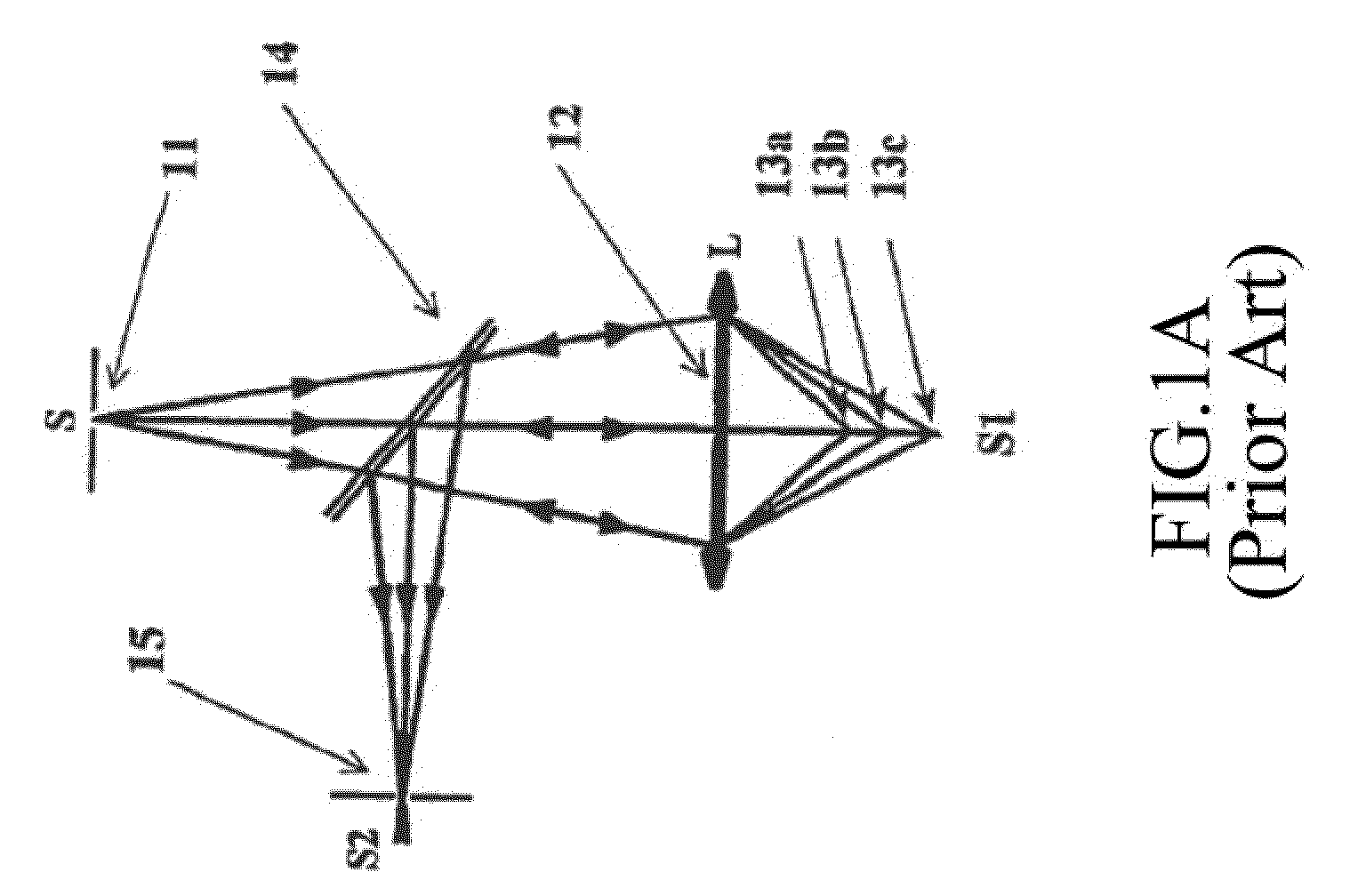
Since such an optical setup of point light field is absolutely blind for all the space except for the sharply focused second point 13, one inspection can only inspect one single dot on the wafer surface that the process for inspection the whole surface of the inspected wafer can be very time consuming and thus might cause the production yield of wafer manufacturing to drop significantly.
Similarly, since the polychromatic light is modulated into a spectral spread light field, where the focal point of the projected light varies according to wavelength, one inspection using the aforesaid confocal microscope can only inspect one single dot on the measured object that the process for inspection the whole surface of the measured object can be very time consuming and thus might cause the production efficiency to drop significantly, and also since only one color can arrive to the imaging device for imaging at each inspection, the obtained image is monochrome that can simply be detected and analyzed by the use of spectrometer.
Nevertheless, although the aforesaid confocal distance sensor can be adapted for inspecting the surface profile of a measured object, it can also only capable of inspection one single dot on a measured object during one inspection.
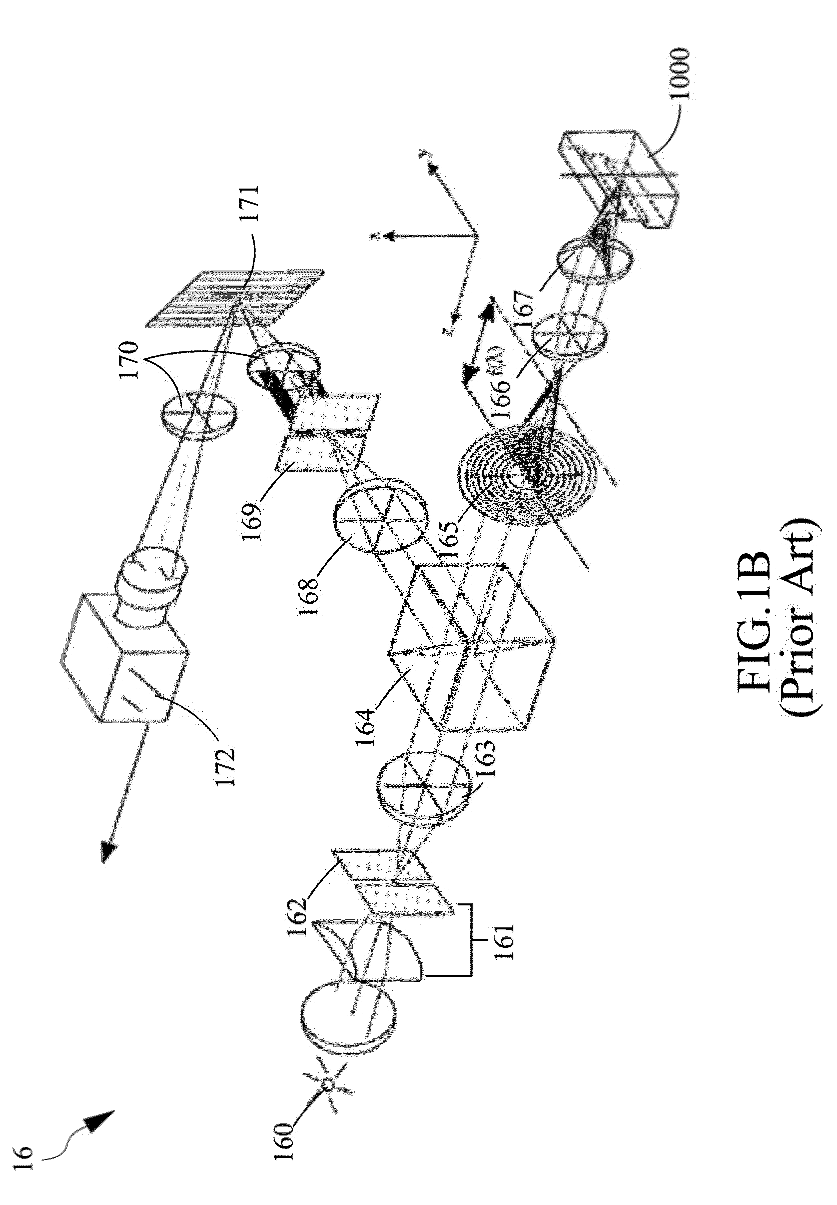
Although the required liner dispersion field can be generated by the DOE, there are a considerable amount of components in the aforesaid optical device that not only it is very complex and bulky in view of system design, but also it may be very expensive to build.

Method used


Image

  • Slit-scan multi-wavelength confocal lens module and slit-scan microscopic system and method using the same
  • Slit-scan multi-wavelength confocal lens module and slit-scan microscopic system and method using the same
  • Slit-scan multi-wavelength confocal lens module and slit-scan microscopic system and method using the same

Examples


Embodiment Construction

[0032]For your esteemed members of reviewing committee to further understand and recognize the fulfilled functions and structural characteristics of the invention, several exemplary embodiments cooperating with detailed description are presented as the follows.

[0033]Please refer to FIG. 2, which is a schematic diagram showing an embodiment of the invention. In this embodiment, a slit-scan multi-wavelength confocal lens module 2 is provided, which comprises: a linear light source module 20, for providing a linear light field 90; a spatial filter 22; and a chromatic dispersion objective lens 21. There can be various ways for generating the aforesaid linear light field 90 so that the light source module 20 of the present invention is not limited to the aforesaid linear light source module 20 shown in FIG. 2. The linear light source module in FIG. 2 is composed of a light source 200, a light guide 201, a lens set 202 and a spatial filter 203. The light source 200 is used for providing a...


PUM


Abstract

The present invention provides a slit-scan multi-wavelength confocal lens module, which utilizes at least two lenses having chromatic aberration for splitting a broadband light into continuously linear spectral lights having different focal length respectively. The present invention utilizes the confocal lens module employing slit-scan confocal principle and chromatic dispersion techniques and the confocal microscopy with optical sectioning ability and high resolution in spectral dispersion to establish a confocal microscopy method and system with long DOF and high resolution, capable of modulating a broadband light to produce the axial chromatic dispersion and focus on different depths toward an object's surface for obtaining the reflected light spectrum from the surface. Thereafter, the spectrum is spatially filtered by a slit and then a peak position with respect to the filtered spectrum along the scanning line is detected by a spectral image sensing unit for generating the sectional profile of the measured surface.

Description

FIELD OF THE INVENTION[0001]The present invention relates to a three-dimensional optical surface profilometry technique, and more particularly, to a slit scan lens module and microscopic system and method having capability of long depth-of-field (DOF) and high resolution by means of combining slit-scan confocal principle and broadband chromatic dispersion technique.BACKGROUND OF THE INVENTION[0002]In the industries utilizing high precision microstructure processing such as IC industry, semiconductor industry, LCD industry, automation industry, electro-optical measurement industry, and so on, a three-dimensional surface profile measurement is always the key procedure required for ensuring the consistency of their manufacturing process. Among all those currently available surface profile measurement techniques, the most commonly used are those optical or electro-optical measuring methods since they can perform a surface profile measuring process in an non-contact manner for accurately...

Claims


Application Information

Patent Timeline
Patent Type & Authority Applications(United States)
IPC IPC(8): G02B21/06G02B3/00
CPCG02B21/0032G02B21/00G02B21/0064
Inventor CHEN, LIANG-CHIACHEN, CHAO-NANCHANG, YI-WEI
Owner NAT TAIPEI UNIV OF TECH
Why Eureka
Eureka Blog
Learn More