Non-volatile memory cell and fabrication method thereof

a technology of memory cells and fabrication methods, applied in the direction of digital storage, instruments, electrical equipment, etc., can solve the problems of significant differences in the wording voltage and current between different memory cells, voltage and metal materials, etc., and achieve the effect of increasing the uniformity of controlling different memory cells

Active Publication Date: 2010-08-05
NAN YA TECH
View PDF2 Cites 100 Cited by
  • Summary
  • Abstract
  • Description
  • Claims
  • Application Information

AI Technical Summary

Benefits of technology

[0006]A resistive memory cell with a specific structure is proposed in the present invention. Because of the specific structure, which limit the surface of the cathode to a small region, which may have a largest electrical field, the metal atoms are expected to initiate the deposition from the small region; accordingly, the time and the resources, such as the metal materials, for forming the metal channel is conserved and thereby the uniformity of controlling different memory cells is increased.

Problems solved by technology

During the formation of the metal channel, too many and too large dendrite structures 13 formed in the solid electrolyte 12 all cause the consumptions of voltage and metal materials.
Furthermore, the differential growth rates of the metal channels between different memory cells cause the significant differences in the wording voltages and currents between different memory cells.

Method used


Image

  • Non-volatile memory cell and fabrication method thereof
  • Non-volatile memory cell and fabrication method thereof
  • Non-volatile memory cell and fabrication method thereof

Examples


first embodiment

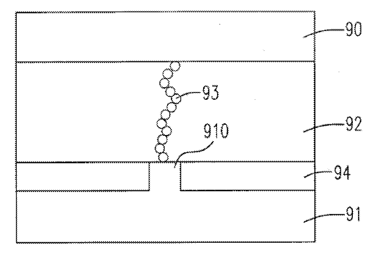
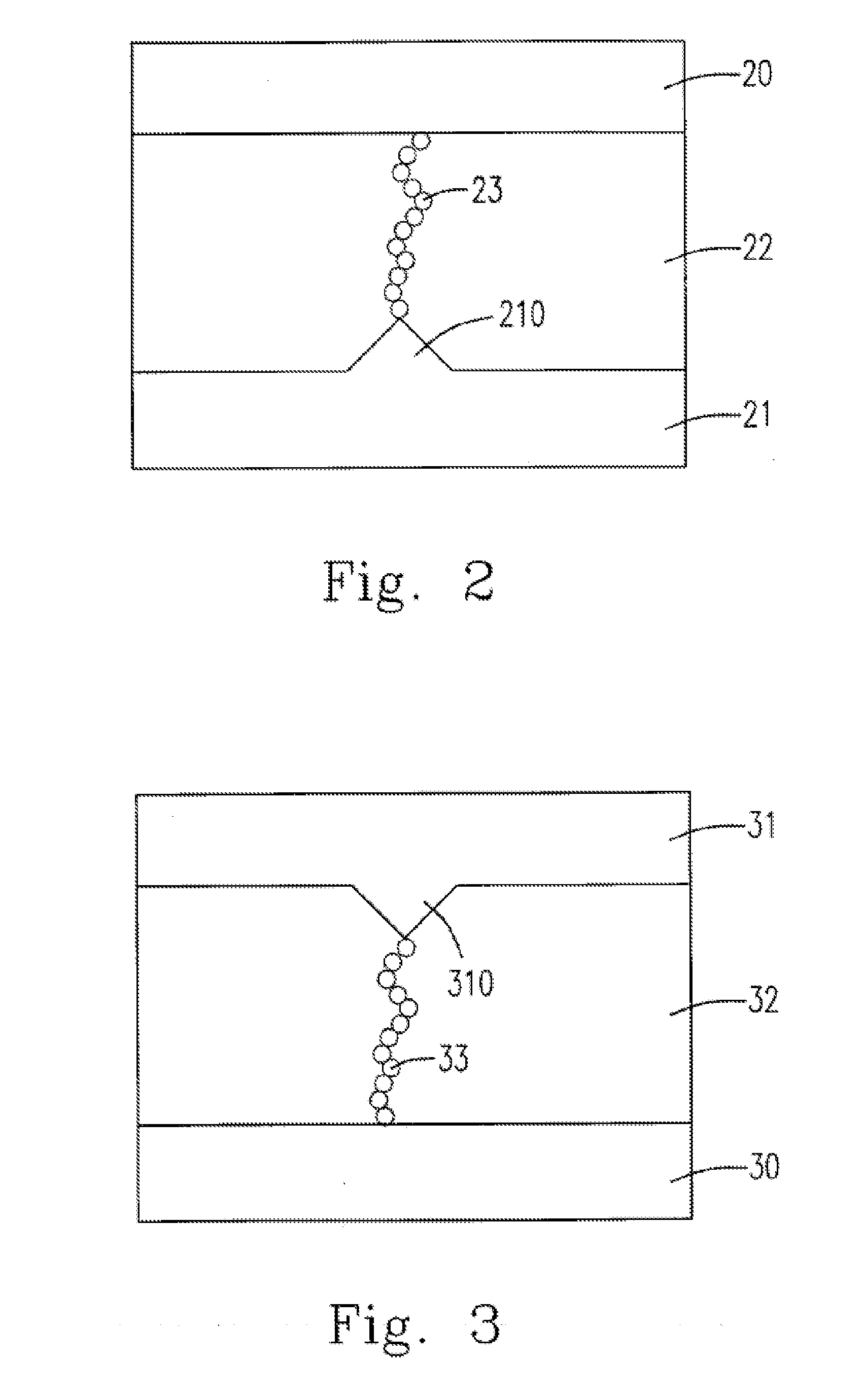
[0051]Please refer to FIG. 2, which is a diagram showing the side view of a non-volatile memory cell according to the present invention. As shown in FIG. 2, the top electrode is an oxidizable electrode 20 where the oxidation and the reduction reactions will take place when a sufficient working voltage is applied thereto, the bottom electrode is an inert electrode 21, and what is deposited between the top and the bottom electrodes is an ion conductor 22. The inert electrode 21 has a bulging terminal 210, which is a closest area to the oxidizable electrode 20, on a surface facing the oxidizable electrode 20. The surface area of the bulging terminal 210 contacting with the ion conductor 22 is smaller than the remaining area of the abovementioned surface facing the oxidizable electrode 20. During the writing process, the oxidizable electrode 20 is an anode and the inert electrode 21 is a cathode. When a sufficient negative voltage is supplied to the inert electrode 21, since the bulging...

second embodiment

[0054]Please refer to FIGS. 4A-4E, which are diagrams showing a fabrication method of the present invention. As shown in FIGS. 4A-4E, simplified plane processes are provided for fabricating the non-volatile memory cell of the present invention. At first, a patterned structure composed of an oxidizable electrode 30, an ion conductor 32, a hard mask 34 and a photoresist layer 35 is formed (shown in FIG. 4A), wherein the patterning process includes lithography and etching processes for transferring a predefined pattern to the abovementioned structure. The lithography process includes the coating of the photoresist layer 35, the soft baking, the mask align, the exposure, the post exposure baking, the development, the hard baking, and the dissolution of the photoresist layer 35. The etching process could be a wet etching, a dry etching, a reactive ion-beam etching or other suitable etching processes. The hard mask 34 is a silicon oxide layer, a silicon nitride layer, a silicon oxynitride...

third embodiment

[0055]Please refer to FIGS. 5A-5E, which are diagrams showing a fabrication method of the present invention. As shown in FIG. 5A, first of all, an oxide layer 53 is deposited on an inert electrode 51 serving as the bottom electrode and merely covers partial of the top surface of the inert electrode 51. Afterward, a metal layer 54 having a material the same as that of the inert electrode 51 is deposited on the structure disclosed in FIG. 5A by a suitable deposition process and covers all exposed portions of the oxide layer 53 and the uncovered top surface of the inert electrode 51 (as shown in FIG. 5B). Subsequently, after the metal layer 54 is etched back by using a back-etching method, portions of the metal layer 54 remain on the sidewalls of the exposed oxide layer 53 (as shown in FIG. 5C), wherein the back-etching method is an anisotropic etching method, e.g. the dry etching including plasma etching, reactive ion etching and so on. Subsequently, the procedure of removing the oxid...


PUM


Abstract

A non-volatile memory cell and a fabrication method thereof are provided. The non-volatile memory cell includes an anode; a cathode having a surface facing the anode; a specific structure disposed on the surface; and an ion conductor disposed among the anode, the cathode and the specific structure, wherein the specific structure is one of a bulging area on the surface of the cathode and an insulating layer with an opening.

Description

FIELD OF THE INVENTION[0001]The present invention relates to a non-volatile memory cell and fabrication method thereof, and more particularly to a resistive non-volatile memory cell and fabrication method thereof.BACKGROUND OF THE INVENTION[0002]Resistive random-access memory (RRAM) has the potential to become the front runner among other non-volatile memories because of the benefits of the high-capacity, the fast switching speeds, the endurance of 1 billion write / read cycles, the lower currents and voltages, and the simpler and smaller cell structure.[0003]Conductive-bridging random access memory (CBRAM) is one of the noticed non-volatile memories. The basic memory cell of CBRAM is composed of a solid electrolyte, e.g. Ag—Ge—Se and Cu / WO3, sandwiched between two metal layers to form a programmable structure. Through the presence or absence of a metal channel formed in the solid electrolyte resulted from the reduction or the oxidation reactions of the metal ions in the solid electro...

Claims


Application Information

Patent Timeline
Patent Type & Authority Applications(United States)
IPC IPC(8): H01L47/00H01L21/326
CPCH01L45/085H01L45/1246H01L45/1253H01L45/1266H01L45/1675H01L45/143H01L45/145H01L45/146H01L45/1273H10N70/245H10N70/828H10N70/8416H10N70/826H10N70/8418H10N70/8825H10N70/8833H10N70/883H10N70/011H10N70/063
Inventor HSIEH, CHUN-ITSAI, SHIH-SHUWU, CHANG-RONG
Owner NAN YA TECH
Why Eureka
Try Eureka