Three-Dimensional Array of Re-Programmable Non-Volatile Memory Elements Having Vertical Bit Lines and a Single-Sided Word Line Architecture

a memory element and array technology, applied in the field of structure, can solve the problems of large power supply, unsatisfactory leakage current, and difficulty in accurately reading the state of addressed (selected) memory elements, and achieve the effects of exceeding reasonable power supply capabilities, accurately reading the state, and reducing the level of leakage current passing through unadressed elements

Active Publication Date: 2010-10-14
SANDISK TECH LLC
View PDF56 Cites 175 Cited by
  • Summary
  • Abstract
  • Description
  • Claims
  • Application Information

AI Technical Summary

Benefits of technology

[0012]The resistance of the memory element, and thus its detectable storage state, can be repetitively set from an initial level to another level and then re-set back to the initial level. For some materials, the amount or duration of the voltage, current, electric field, heat and the like applied to change its state in one direction is different (asymmetrical) with that applied to change in another direction. With two detectable states, each memory element stores one-bit of data. With the use of some materials, more than one bit of data may be stored in each memory element by designating more than two stable levels of resistance as detectable states of the memory element. The three-dimensional array architecture herein is quite versatile in the way it may be operated.
[0013]This three-dimensional architecture also allows limiting the extent and number of unaddressed (non-selected) resistive memory elements across which an undesired level of voltage is applied during reading and programming operations conducted on other addressed (selected) memory elements. The risk of disturbing the states of unaddressed memory elements and the levels of leakage current passing through unaddressed elements may be significantly reduced from those experienced in other arrays using the same memory element material. Leakage currents are undesirable because they can alter the apparent currents being read from addressed memory elements, thereby making it difficult to accurately read the states of addressed (selected) memory elements. Leakage currents are also undesirable because they add to the overall power draw by an array and therefore undesirably causes the power supply to have to be made larger than is desirable. Because of the relatively small extent of unaddressed memory elements that have voltages applied during programming and reading of addressed memory elements, the array with the three-dimensional architecture herein may be made to include a much larger number of memory elements without introducing errors in reading and exceeding reasonable power supply capabilities.
[0014]In addition, the three-dimensional architecture herein allows variable resistance memory elements to be connected at preferably orthogonal crossings of bit and word line conductors without the need for diodes or other non-linear elements being connected in series with the variable resistive elements. In existing arrays of variable resistance memory elements, a diode is commonly connected in series with each memory element in order to reduce the leakage current though t

Problems solved by technology

Leakage currents are undesirable because they can alter the apparent currents being read from addressed memory elements, thereby making it difficult to accurately read the states of addressed (selected)

Method used


Image

  • Three-Dimensional Array of Re-Programmable Non-Volatile Memory Elements Having Vertical Bit Lines and a Single-Sided Word Line Architecture
  • Three-Dimensional Array of Re-Programmable Non-Volatile Memory Elements Having Vertical Bit Lines and a Single-Sided Word Line Architecture
  • Three-Dimensional Array of Re-Programmable Non-Volatile Memory Elements Having Vertical Bit Lines and a Single-Sided Word Line Architecture

Examples


Embodiment Construction

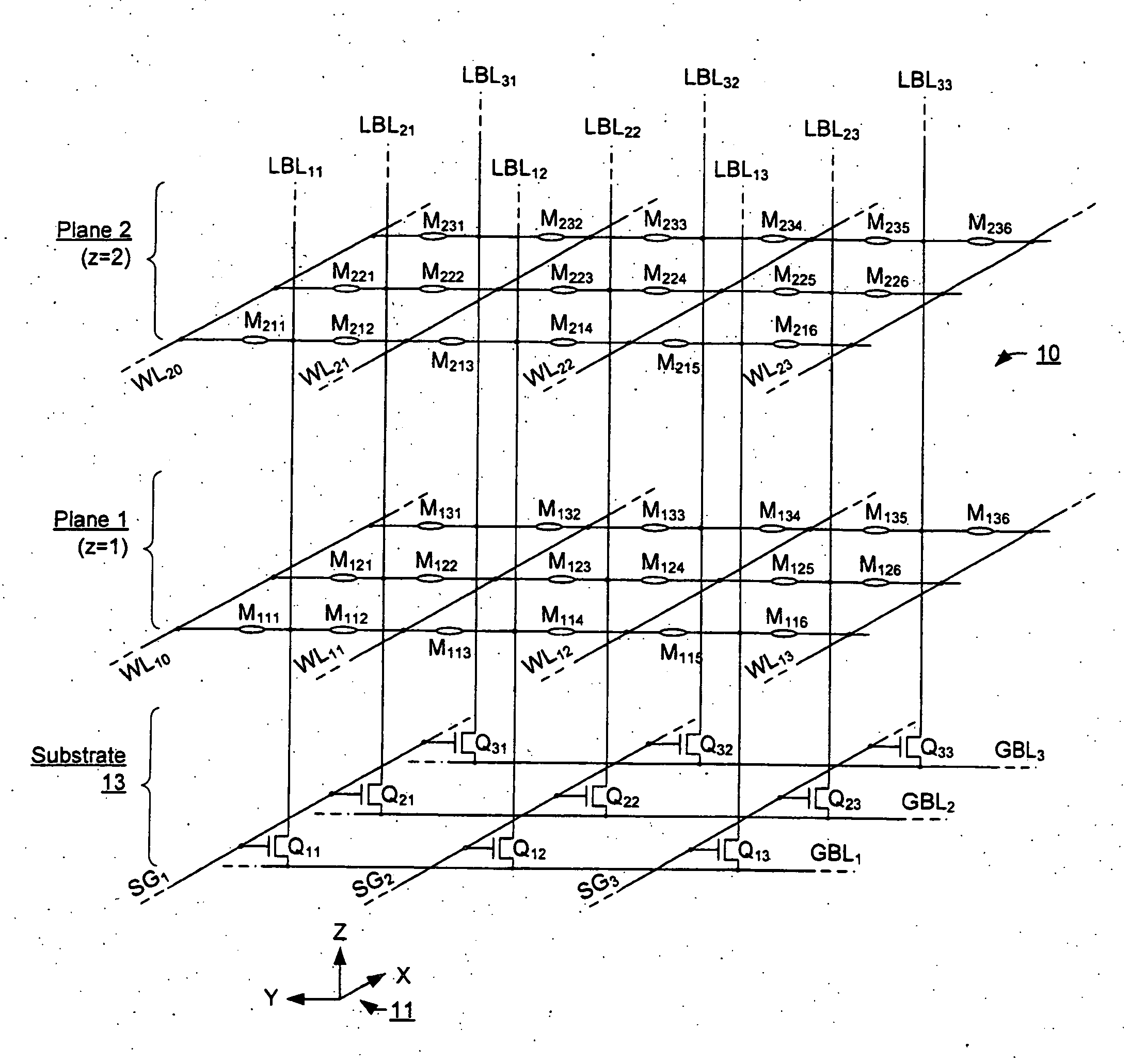
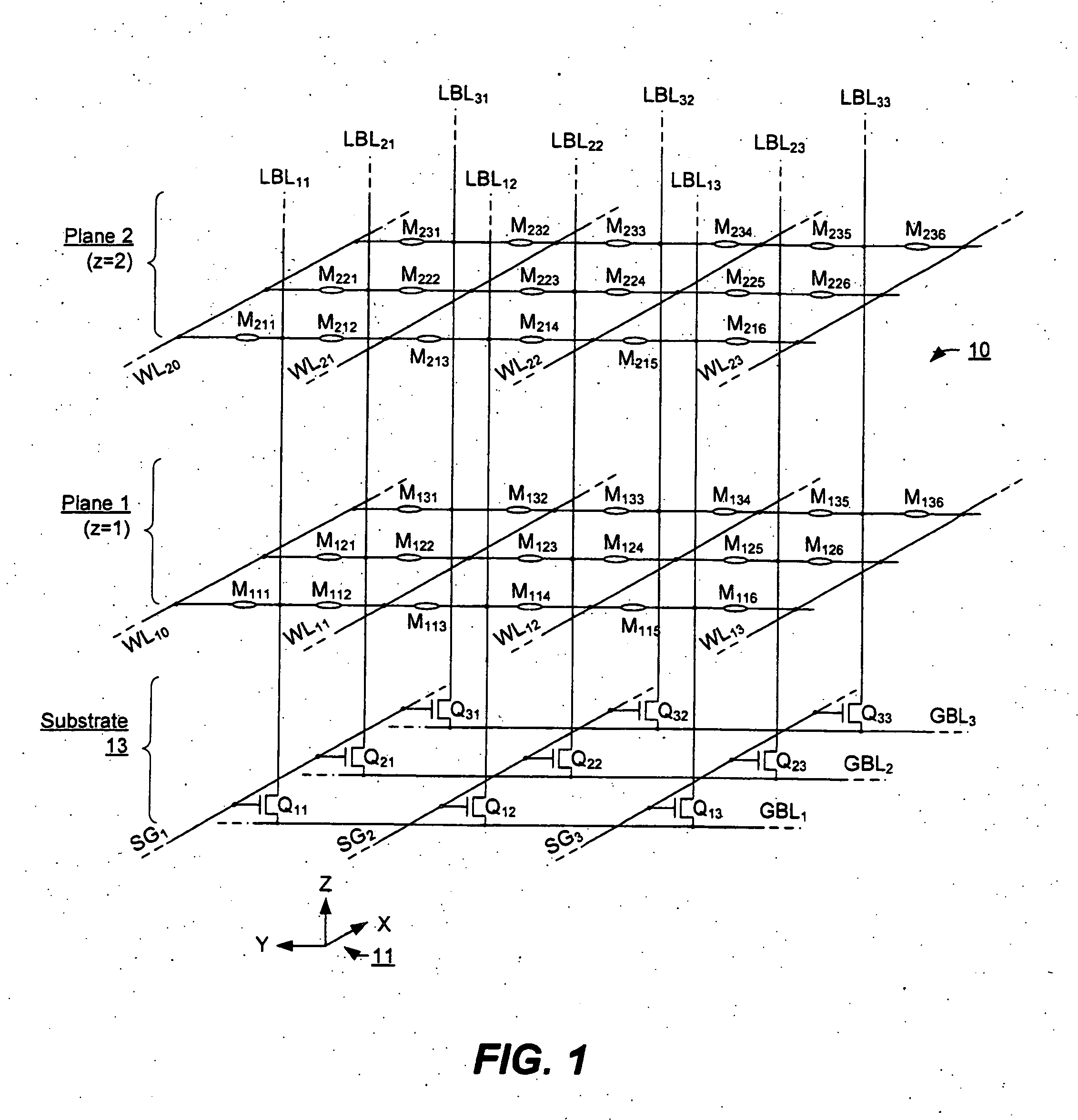
[0038]Referring initially to FIG. 1, an architecture of a three-dimensional memory 10 is schematically and generally illustrated in the form of an equivalent circuit of a portion of such a memory. This is a specific example of the three-dimensional array summarized above. A standard three-dimensional rectangular coordinate system 11 is used for reference, the directions of each of vectors x, y and z being orthogonal with the other two.

[0039]A circuit for selectively connecting internal memory elements with external data circuits is preferably formed in a semiconductor substrate 13. In this specific example, a two-dimensional array of select or switching devices Qxy are utilized, where x gives a relative position of the device in the x-direction and y its relative position in the y-direction. The individual devices Qxy may be a select gate or select transistor, as examples. Global bit lines (GBLx) are elongated in the y-direction and have relative positions in the x-direction that ar...


PUM


Abstract

A three-dimensional array especially adapted for memory elements that reversibly change a level of electrical conductance in response to a voltage difference being applied across them. Memory elements are formed across a plurality of planes positioned different distances above a semiconductor substrate. A two-dimensional array of bit lines to which the memory elements of all planes are connected is oriented vertically from the substrate and through the plurality of planes. A single-sided word line architecture provides a word line exclusively for each row of memory elements instead of sharing one word line between two rows of memory elements thereby avoids linking the memory element across the array across the word lines. While the row of memory elements is also being accessed by a corresponding row of local bit lines, there is no extension of coupling between adjacent rows of local bit lines and therefore leakage currents beyond the word line.

Description

CROSS-REFERENCE TO RELATED APPLICATIONS[0001]This application is a continuation-in-part of U.S. application Ser. No. 12 / 420,334 filed on Apr. 8, 2009.BACKGROUND[0002]The subject matter of this application is the structure, use and making of re-programmable non-volatile memory cell arrays, and, more specifically, to three-dimensional arrays of memory storage elements formed on semiconductor substrates.[0003]Uses of re-programmable non-volatile mass data storage systems utilizing flash memory are widespread for storing data of computer files, camera pictures, and data generated by and / or used by other types of hosts. A popular form of flash memory is a card that is removably connected to the host through a connector. There are many different flash memory cards that are commercially available, examples being those sold under trademarks CompactFlash (CF), the MultiMediaCard (MMC), Secure Digital (SD), miniSD, microSD, Memory Stick, Memory Stick Micro, xD-Picture Card, SmartMedia and Tra...

Claims


Application Information

Patent Timeline
IPC IPC(8): G11C5/02G11C7/00
CPCB82Y10/00G11C11/06035G11C11/5678G11C11/5685G11C13/0004G11C13/0007G11C13/0011G11C13/003G11C13/004G11C13/0064G11C13/0069G11C13/025G11C2013/0045G11C2013/0088G11C2213/19G11C2213/32G11C2213/34G11C2213/71G11C2213/78H01L27/2409H01L27/2436H01L27/249H01L45/06H01L45/065H01L45/08H01L45/085H01L45/1226H01L45/1266H01L45/142H01L45/143H01L45/146H01L45/148H01L45/149G11C16/10G11C11/5614H10B63/30H10B63/845H10N70/235H10N70/24H10N70/245H10N70/823H10N70/8416H10N70/231H10N70/8822H10N70/8825H10N70/884H10N70/8845H10N70/8833H10B63/20H10B63/84H10N70/826H10N70/841G11C2213/55G11C2213/75H01L23/528
Inventor YAN, TIANHONGSAMACHISA, GEORGE
Owner SANDISK TECH LLC
Why Eureka
Try Eureka