Micro-pixel ultraviolet light emitting diode

a technology of ultraviolet light and diodes, which is applied in the manufacture of semiconductor/solid-state devices, semiconductor devices, electrical devices, etc., can solve the problems of high method undesirable, limited array size, and insufficient structure, so as to reduce defects, reduce strain, and relieve strain

Active Publication Date: 2010-10-21
NIITEK
View PDF5 Cites 38 Cited by
  • Summary
  • Abstract
  • Description
  • Claims
  • Application Information

AI Technical Summary

Benefits of technology

[0021]A feature of the present invention is that the buffer layer of the present invention can be either a single III-Nitride layer that is not thin (thickness>0.1 μm) for AlN, or comprises ternary (AlGaN, AlInN), quaternary (AlInGaN) or multiple layers of III-Nitride, preferably made of AlInGaN and containing a design optimized for both strain relief and optical transparency. In the prior art, the buffer layer comprises thin AlN in a single layer. Another feature is the use of the superlattice for both reducing defects and relieving strain. A superlattice is a series of thin layers of alternating composition that serves as a transducer from a lower layer to an upper layer, relieving str

Problems solved by technology

This method is highly undesirable due to the large number of connections and the cost associated with assembly.
As the aluminum content increases, such as in AlxGa1-xN, the resistance in the layer increases thereby rendering the structure insufficient.
Even without aluminum the size of the array is limited since resistance in the n-type layer prohibits an extensive path length for current flow.
Group III nitride LEDs are difficult to manufacture for a number of reasons.
For example, defects arise from lattice and thermal mismatch between the group III-Nitride based semiconductor layers and a substrate such as sapphire, silicon carbide, or silicon on which they are constructed.
In addition, impurities and tilt boundaries result in the formation of crystalline defects.
These defects have been shown to reduce the efficiency and lifetime of LEDs and LDs fabricated from these materials.
This method, however, has been shown to be ineffective for the growth of aluminum-co

Method used


Image

  • Micro-pixel ultraviolet light emitting diode
  • Micro-pixel ultraviolet light emitting diode
  • Micro-pixel ultraviolet light emitting diode

Examples


Embodiment Construction

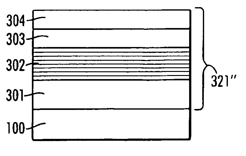
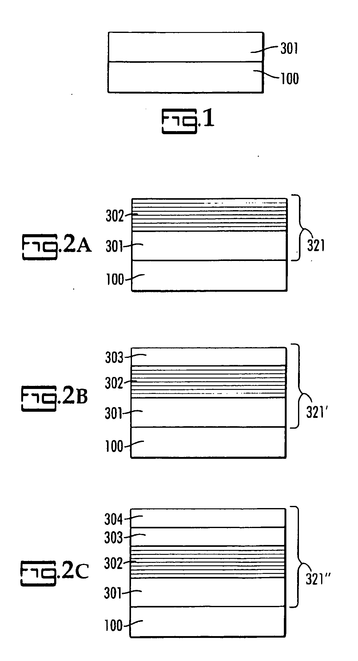
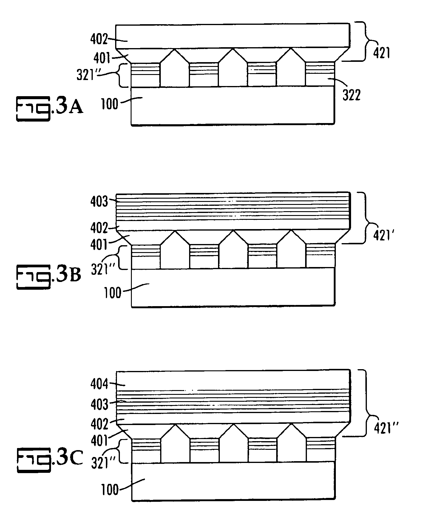
[0039]The present invention is an array of light-emitting devices (LED) and a method for making an array of LED's, particularly one that emits deep ultraviolet light. In particular, a template, 10, is provided that serves as a platform for an array of ultraviolet light-emitting structures, 12, as shown in FIG. 4. Briefly, template 10 includes a substrate, and a first buffer layer added onto the substrate as the first step in forming the LED wafer.

[0040]The template may include a substrate but has two buffer layers, one of which is trenched and the second of which preferably forms a coalesced planar layer over the first. The coalescing involves performing PLOG over deep trenches (height 0.4 μm in case of AlN), or over shallow or deep trenches if the pillars encompass more than one group III species or a combination of multiple layers. The pillars may comprise a multi-layer stack of III-Nitride based semiconductors including AlN, and a strain-relieving superlattice in an array. In som...


PUM


Abstract

An ultra-violet light-emitting diode (LED) array, 12, and method for fabricating same with an AlInGaN multiple-quantum-well active region, 500, exhibiting stable cw-powers. The LED includes a template, 10, with an ultraviolet light-emitting array structure on it. The template includes a first buffer layer, 321, then a second buffer layer, 421, on the first preferably with a strain-relieving layer in both buffer layers. Next there is a semiconductor layer having a first type of conductivity, 500, followed by a layer providing a quantum-well region, 600, with an emission spectrum ranging from 190 nm to 369 nm. Another semiconductor layer having a second type of conductivity is applied next, 800. A first metal contact, 980, is a charge spreading layer in electrical contact with the first layer and between the array of LED's. A second contact, 990, is applied to the semiconductor layer having the second type of conductivity, to complete the LED.

Description

CROSS-REFERENCE TO RELATED APPLICATIONS[0001]The present application claims priority to PCT / US07 / 81625 filed Oct. 7, 2007 which, in turn, claims benefit to expired U.S. Provisional Appl. No. 60 / 852,673 filed Oct. 18, 2006 both of which are incorporated by reference. The present application also claims benefit to pending U.S. Provisional Appl. No. 60 / 935,491 filed Aug. 14, 2007 which is incorporated by reference.BACKGROUND OF THE INVENTION[0002]The present invention relates generally to a micro-pixel ultraviolet light-emitting device and method of manufacturing a light-emitting device.[0003]Group III nitride compound semiconductors such as, for instance, gallium nitride (GaN), aluminum nitride (AlN), indium nitride (InN) (hereinafter also referred to as a “Group III-nitride semiconductor” or “III-nitrides”) have been gaining attention as a material for semiconductor devices that emit green, blue or ultraviolet light. A light-emitting diode or a laser diode that emits blue light may b...

Claims


Application Information

Patent Timeline
IPC IPC(8): H01L33/04H01L33/00H01L33/12H01L33/32
CPCH01L27/156H01L33/32H01L33/12
Inventor ADIVARAHAN, VINODKHAN, ASIFKHAN, RUBINA
Owner NIITEK
Why Eureka
Try Eureka