Method for manufacturing semiconductor device

a semiconductor device and manufacturing method technology, applied in the field of lithography technique, can solve the problems of reducing the exposure contrast and the exposure latitude, affecting the quality of semiconductor devices, etc., and achieves the effect of reducing the flare generated at the time of exposing the mask, densely integrated semiconductors, and high exposure latitud

Active Publication Date: 2010-11-11
RENESAS ELECTRONICS CORP
View PDF14 Cites 9 Cited by
  • Summary
  • Abstract
  • Description
  • Claims
  • Application Information

AI Technical Summary

Benefits of technology

[0031]According to the embodiment, an effect of flare generated at the time of exposing a mask can be reduced, and a fine wiring p...

Problems solved by technology

In the EUV lithography, since the wavelength of the exposure light is quite short and an optical system including a mask is of reflective type, there is problematic flare which can be a source of stray light caused by that the exposure light is scattered toward undesired directions.
While the flare can be classified into several groups, an e...

Method used


Image

  • Method for manufacturing semiconductor device
  • Method for manufacturing semiconductor device
  • Method for manufacturing semiconductor device

Examples


embodiment 1

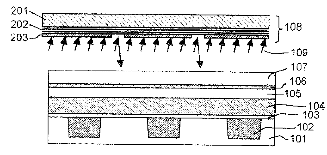
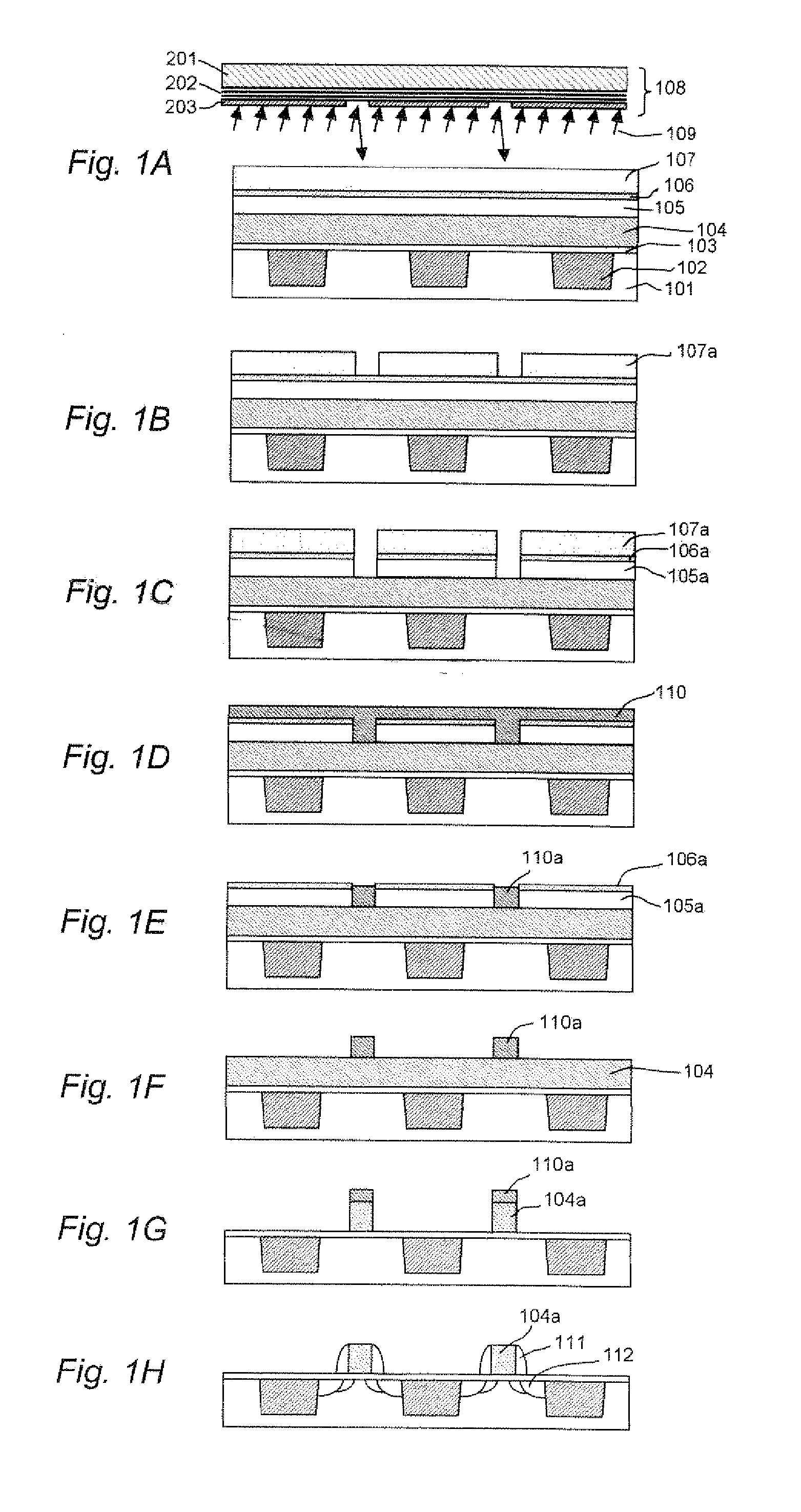
[0042]FIG. 1A to FIG. 1H are explanatory views showing an example of a method for manufacturing a semiconductor device, according to the present invention. Here, they are partial cross-sectional views of a semiconductor integrated circuit in which a number of transistor elements (e.g., MOSFET) are formed in a semiconductor substrate, and a wiring pattern including a gate electrode of each element and a gate wiring connected to the gate electrode is formed thereon.

[0043]First, as shown in FIG. 1A, an isolation 102 for isolating respective elements is formed beforehand in a semiconductor substrate 101 formed of, e.g., Si (silicon). On the substrate 101, a gate oxide film 103, an electrically conductive film 104, hard coating films 105 and 106, and a positive resist 107 are sequentially formed.

[0044]The gate oxide film 103 can be formed of SiO2 or a high-dielectric (high-k) material such as HfSiO (hafnium silicate), HfAlON (nitrogen added hafnium aluminate), HfO2, or Y2O3. The conducti...

embodiment 2

[0068]FIG. 3A to FIG. 3J are explanatory views showing another example of a method for manufacturing a semiconductor device, according to the present invention. Here, they are partial cross-sectional views of a semiconductor integrated circuit in which a number of transistor elements (e.g., MOSFET) are formed in a semiconductor substrate, and a wiring pattern including a gate electrode of each element and a gate wiring connected to the gate electrode is formed thereon.

[0069]According to this embodiment, a gate having an extremely thin line width is formed with a high degree of dimensional accuracy by performing a gate thinning process called slimming.

[0070]First, as shown in FIG. 3A, an isolation 102 for isolating respective elements is formed beforehand in a semiconductor substrate 101 formed of, e.g., Si (silicon). On the substrate 101, a gate oxide film 103, an electrically conductive film 104, an underlying film 130, hard coating films 131 and 132, and a positive resist 133 are ...

embodiment 3

[0091]FIG. 4A to FIG. 4F are explanatory views showing still another example of a method for manufacturing a semiconductor device, according to the present invention. Here, they are partial cross-sectional views of a semiconductor integrated circuit in which a number of transistor elements (MOSFET, for example) are formed in a semiconductor substrate, and a wiring pattern including a gate electrode of each element and a gate wiring connected to the gate electrode is formed thereon.

[0092]According to this embodiment, once a reversed pattern is made by combining a negative exposure mask of a wiring pattern with a positive resist, and then a wiring pattern is formed in an opening part of the reversed pattern, thereby a gate having an extremely fine minimum line width can be formed with a high degree of dimensional accuracy.

[0093]First, as shown in FIG. 4A, an isolation 102 for isolating respective elements is formed beforehand in a semiconductor substrate 101 formed of, e.g., Si (silic...


PUM


Abstract

A reverse pattern is formed once by combining a negative exposure mask having a wiring pattern with a positive resist, and then a positive wiring pattern is formed by use of the reverse pattern. That is, a positive resist applied on a semiconductor substrate is exposed by use of the exposure mask having an opening part in a region corresponding to the wiring pattern, and then the exposed part is removed by development to form a resist pattern, thereby forming the wiring pattern in the region corresponding to the opening part of the resist pattern. Consequently, it is hardly affected by flare during EUV exposure, thereby fabricating a fine wiring pattern with higher exposure latitude.

Description

TECHNICAL FIELD[0001]The present invention relates to a lithography technique used in manufacturing a semiconductor device such as semiconductor integrated circuit, more particularly, to a technique to fabricate a fine gate with a high degree of dimension accuracy.BACKGROUND[0002]The lithography technique is employed for a method of transferring a fine pattern onto a substrate during processes of manufacturing a semiconductor integrated circuit. A projection aligner is very often used in the lithography technique, wherein the pattern can be transferred by irradiating a resist formed on the substrate with exposure light transmitted through a photomask mounted on the projection aligner.[0003]In recent years, it is increasingly demanded that the device be more densely integrated and an operation speed be increased, and researches for pattern miniaturization are under way to meet these demands. In order to meet these demands for miniaturization, an effort has been made to improve a reso...

Claims


Application Information

Patent Timeline
IPC IPC(8): G03F7/20
CPCH01L21/0337H01L21/28123H01L21/32139H01L21/823437H01L21/823475H01L29/66545H01L21/823871H01L27/0207H01L28/20H01L29/517H01L21/823828
Inventor TANAKA, TOSHIHIKO
Owner RENESAS ELECTRONICS CORP
Why Eureka
Try Eureka