Inverter topologies usable with reactive power

a technology of reactive power and inverter, which is applied in the direction of electronic switching, dc-ac conversion without reversal, pulse technique, etc., can solve the problems of high switching loss, poor recovery behavior of internal antiparallel body diodes, and high frequency ringing, and achieve high efficiency of inverter circuits

Active Publication Date: 2011-01-20
VINCOTECH HLDG R L
View PDF23 Cites 116 Cited by
  • Summary
  • Abstract
  • Description
  • Claims
  • Application Information

AI Technical Summary

Benefits of technology

[0010]The present invention relates to inverter circuits that can be used with reactive loads. An inverter circuit is provided which comprises first and second input terminals for be-ing connected to a DC power source; first and second output terminals for outputting an AC voltage; at least one metal oxide semiconductor field effect transistor, MOSFET, having a parasitic body diode. The inverter circuit further comprises at least one dis-abling element for disabling said body diode. This results in high efficiency of the in-verter circuit in combination with a reactive power capability.
[0014]When decoupling the MOSFET by means of an inductor, also a bypass diode for the reverse path can be advantageous.
[0015]The present invention also relates to a semiconductor switching device, comprising at least one metal oxide semiconductor field effect transistor, MOSFET, having a drain terminal and a source terminal, and at least one insulated gate bipolar transistor, IGBT, having a collector terminal and an emitter terminal, wherein said MOSFET and said IGBT are connected in parallel by coupling the collector terminal of the IGBT to the drain terminal of the MOSFET, and by coupling the emitter terminal of the IGBT to the source terminal of the MOSFET. This structure results in two basic improvements in efficiency:
[0016]Firstly, the efficiency at high load range is enhanced by allocating the static losses of the switch to the IGBT and the dynamic losses to the MOSFET. Secondly, the effi-ciency at light load range can be enhanced by assigning both the static and the switch-ing losses to the MOSFET. The MOSFET turns on fast and is delayed at switch-off so that the switching losses are assigned to the MOSFET. The MOSFET will also carry the current at low power, thus eliminating one pn junction voltage drop of the IGBT, whereas the IGBT will take the majority at maximum load condition. At low load the IGBT is not conducting at all, so resistential tail current losses are eliminated for the whole power range. Therefore it is possible to improve both the overall and the maximum load efficiency.
[0018]The invention minimizes the effect of parasitic body diodes by preventing significant current flow through the internal body diode of MOSFETs present in an inverter circuit. This ensures minimal body diode reverse recovery effects on every switching cycle. The switching circuit is made more robust because of the reduced power loss, which in turn allows for the use of smaller components, smaller filters, less heat sinking and potentially lower total costs.

Problems solved by technology

MOSFETs are generally known to have very good switching performance but the internal antiparallel body diode exhibits poor recovery behavior.
Abrupt reverse recovery of the body diode can cause higher switching losses and high frequency ringing, which places higher stresses on the com-ponents and can couple to the output and can cause noise and electromagnetic inter-ference, EMI, associated problems.
The addition of these diodes significantly increases the cost of the inverter de-sign and adds conduction losses.
IGBTs typically have poorer switching performance than MOSFETs, but require the addition of fewer diodes to pro-vide rapid recovery behavior, since the internal series diode present in IGBTs allows the designer to add a single diode to the free-wheeling path.
The use of IGBTs can reduce the cost of an inverter design but may lower the inverter efficiency at higher frequencies.
Furthermore, when developing highly efficient inverter topologies which can handle reactive power, the intrinsic diode of the MOSFET will cause high reverse recovery losses when reactive power has to be managed. FIG. 12 shows an inverter circuit be-ing formed only by IGBTs which, however, is not fast enough for most novel solar ap-plications.
This com-bined circuit, however, has the disadvantage that in the case of reactive power the intrinsic body diode causes losses which deteriorate the efficiency to an unacceptable extent.
However, these components usually have a higher Rds-on and therefore the losses are significant.
Another disadvantage is that their poor reverse recovery properties lead to an unsatisfactory performance in power factor compensation and bi-directional usage.

Method used


Image

  • Inverter topologies usable with reactive power
  • Inverter topologies usable with reactive power
  • Inverter topologies usable with reactive power

Examples


Embodiment Construction

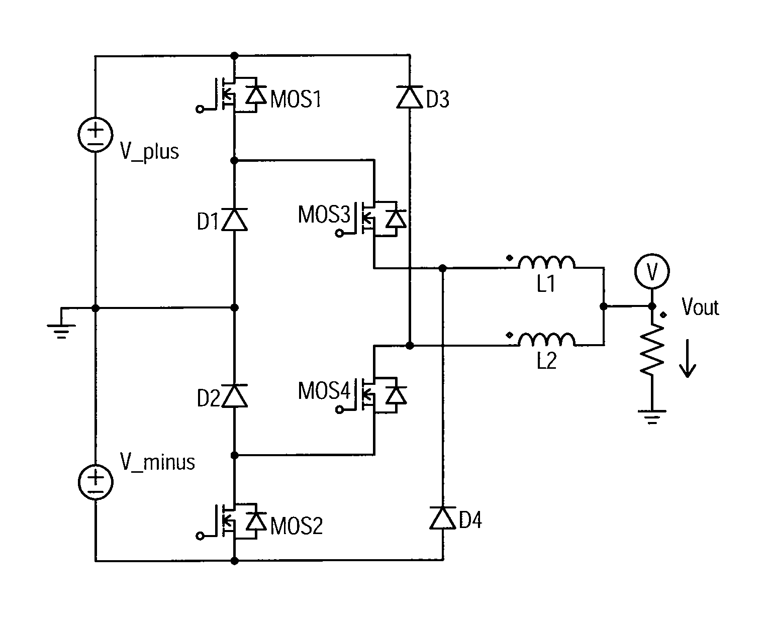
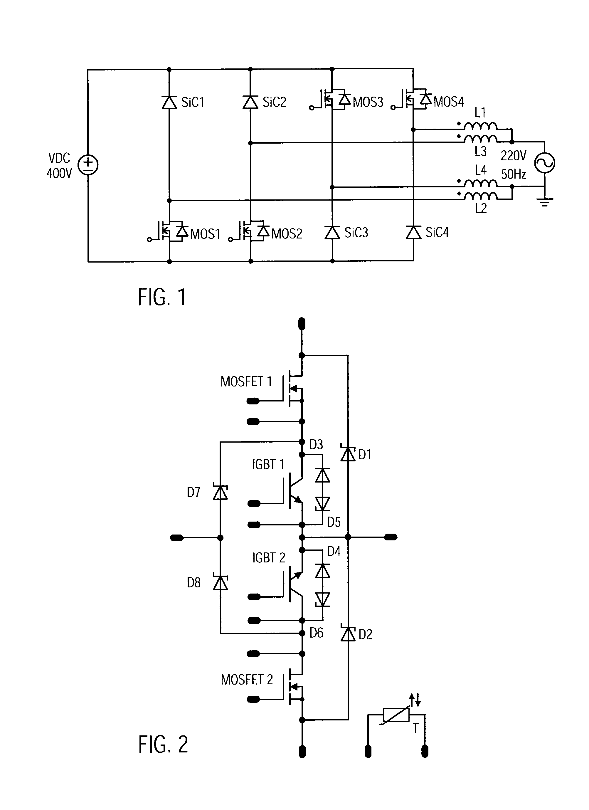
[0034]FIG. 1 shows a highly efficient inverter topology having the ability to handle a reactive load which uses only MOSFET switches in a full bridge configuration. The circuit shown in FIG. 1 is coupled to a 400 Volt DC input as it results for instance from a solar photovoltaic panel. The output can be connected to the 220 Volt AC 50 Hz power grid and tolerates reactive power, even if it is not only necessary for line impedance meas-urements or for the protection of the components at special conditions. The circuit al-lows for full reactive power and enlarges the use as a cos φ compensation of the power grid and also for fully bidirectional applications, such as high-efficiency battery chargers. An excellent efficiency level is reached in both directions when using silicon carbide Schottky diodes.

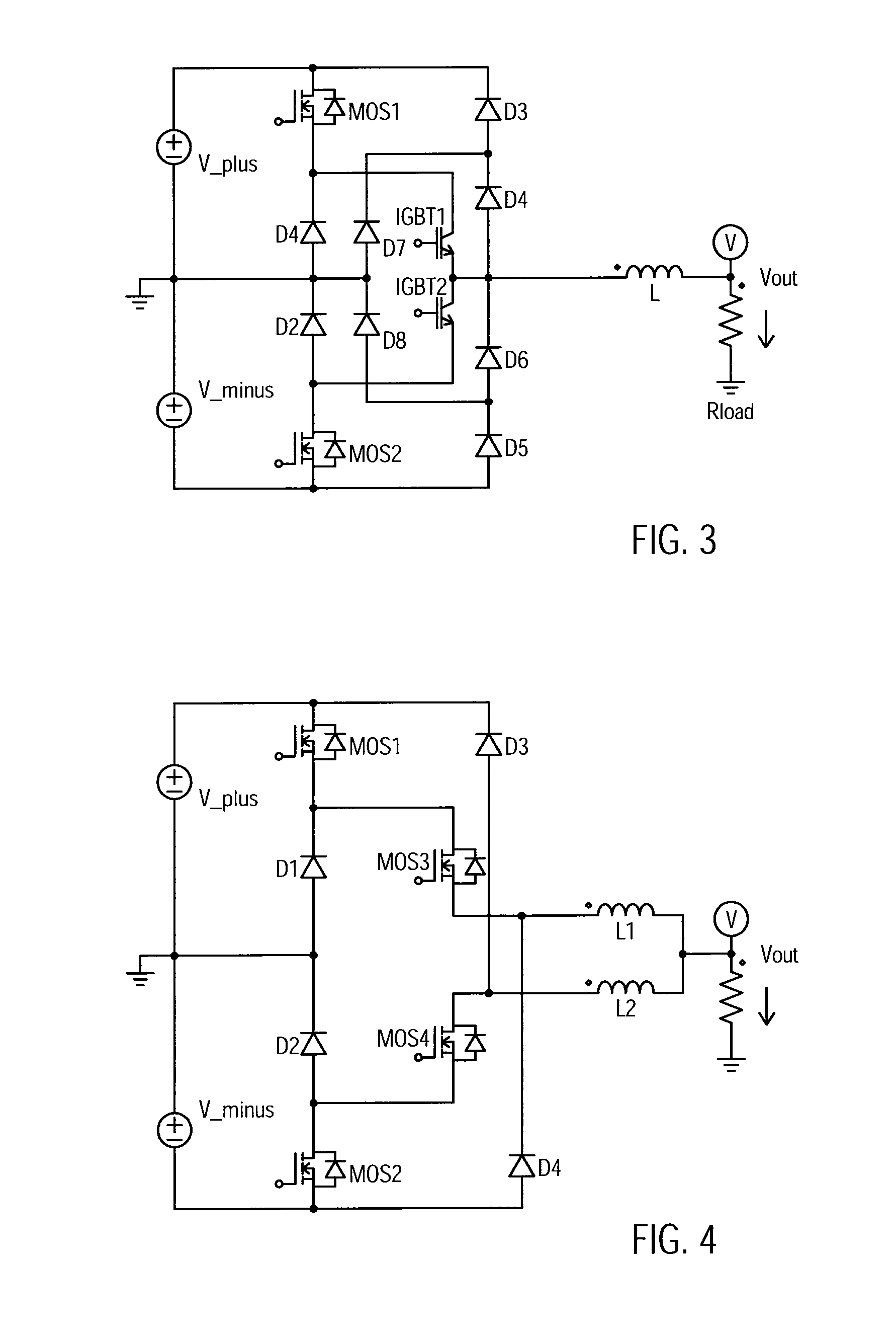
[0035]When referring to FIG. 14, a neutral point clamped, NPC, inverter is shown which uses a mixed chip configuration, i.e. MOSFETs in combination with IGBTs. The NPC in-verter of FIG. 14...


PUM


Abstract

The present invention generally relates to power electronic switching circuits and in particular to inverter modules employing two or more controlled switches that can be used with reactive loads. An inverter circuit is provided which comprises first and second input terminals for being connected to a DC power source; first and second output terminals for outputting an AC voltage; at least one metal oxide semiconductor field effect transistor, MOSFET, having a parasitic body diode. The inverter circuit further comprises at least one disabling element for disabling said body diode. This may result in an improved efficiency of the inverter circuit in combination with a reactive power capability. Further, a semiconductor switching device is disclosed, comprising at least one metal oxide semiconductor field effect transistor, MOSFET, and at least one insulated gate bipolar transistor, IGBT, wherein said MOSFET and said IGBT are connected in parallel.

Description

BACKGROUND OF THE INVENTION[0001]The present invention generally relates to power electronic switching circuits and in particular to inverter modules employing two or more controlled switches.[0002]Efficiency is becoming increasingly important in the field of power electronics and in many applications, such as inverter modules for the solar market, the efficiency optimi-zation turned out to represent a major design goal. Photovoltaic solar panels com-monly use PWM, pulse width modulation, inverters to convert DC power generated by the solar cell into AC power which can be fed into the power grid. Typical further appli-cations of these inverters include their use in uninterruptable power supplies, UPS, fuel cells and wind turbines. Further, PWM inverters may be used to provide compensation for reactive loads, harmonic cancellation of supply grids, or as variable speed drives for induction motors. The most commonly used inverters are one phase and three phase transformerless inverters...

Claims


Application Information

Patent Timeline
Patent Type & Authority Applications(United States)
IPC IPC(8): H02M7/537
CPCH02M7/48H02M7/487H03K17/08142H02J3/383H03K2217/0036Y02E10/563H03K17/6871H02J2300/24H02J3/381Y02E10/56H02M1/0085
Inventor FRISCH, MICHAELTEMESI, ERNO
Owner VINCOTECH HLDG R L
Why Eureka
Try Eureka