

Solid-state imaging device, process of making solid state imaging device, digital still camera, digital video camera, mobile phone, and endoscope
Active Publication Date: 2011-03-03
FUJIFILM CORP
View PDF4 Cites 90 Cited by
- Summary
- Abstract
- Description
- Claims
- Application Information
AI Technical Summary
Benefits of technology
[0188]If desired, the colored thermosetting composition may contain various additives as long as such does not affect the effects of the invention. Examples of additives include binders, curing agents, curing catalysts, solvents, fillers, polymeric compounds other than those described, surfactants, adhesion enhancer, antioxidants, UV absorbers, anti-coagulants, and dispersants.
Problems solved by technology
Therefore, as the pixel pitch reduces, the area ratio of the circuit region in unit pixel becomes larger, which of necessity raises the problem of reduction in the effective area of the photodiode, i.e., reduction of a pixel aperture ratio.
Reduction of aperture ratio leads to reduction of sensitivity.
Method used
View moreImage
Smart ImageViewing Examples

Examples
example 1
[0246]The auxiliary sealing sublayer was a silicon oxide film formed by high frequency magnetron sputtering using silicon oxide as a target at a degree of vacuum of 0.1 Pa in an Ar / O2 atmosphere.
example 2
[0247]The auxiliary sealing sublayer was a silicon nitride film formed by high frequency magnetron sputtering using silicon nitride as a target at a degree of vacuum of 0.1 Pa in an Ar / N2 atmosphere.
example 3
[0248]The auxiliary sealing sublayer was a silicon oxynitride film formed by high frequency magnetron sputtering using silicon oxynitride as a target at a degree of vacuum of 0.1 Pa in an Ar / N2 atmosphere.
Login to View More PUM
 Abstract
A solid-state imaging device includes an array of pixels, each pixel includes: a pixel electrode; an organic layer; a counter electrode; a sealing layer; a color filter; a readout circuit; and a light-collecting unit as defined herein, the photoelectric layer contains an organic p type semiconductor and an organic n type semiconductor, the organic layer further includes a charge blocking layer as defined herein, an ionization potential of the charge blocking layer and an electron affinity of the organic n type semiconductor in the photoelectric layer has a difference of at least 1 eV, and the sealing layer includes a first sealing sublayer formed by atomic layer deposition and a second sealing sublayer formed by physical vapor deposition and containing one of a metal oxide, a metal nitride, and a metal oxynitride.
Description
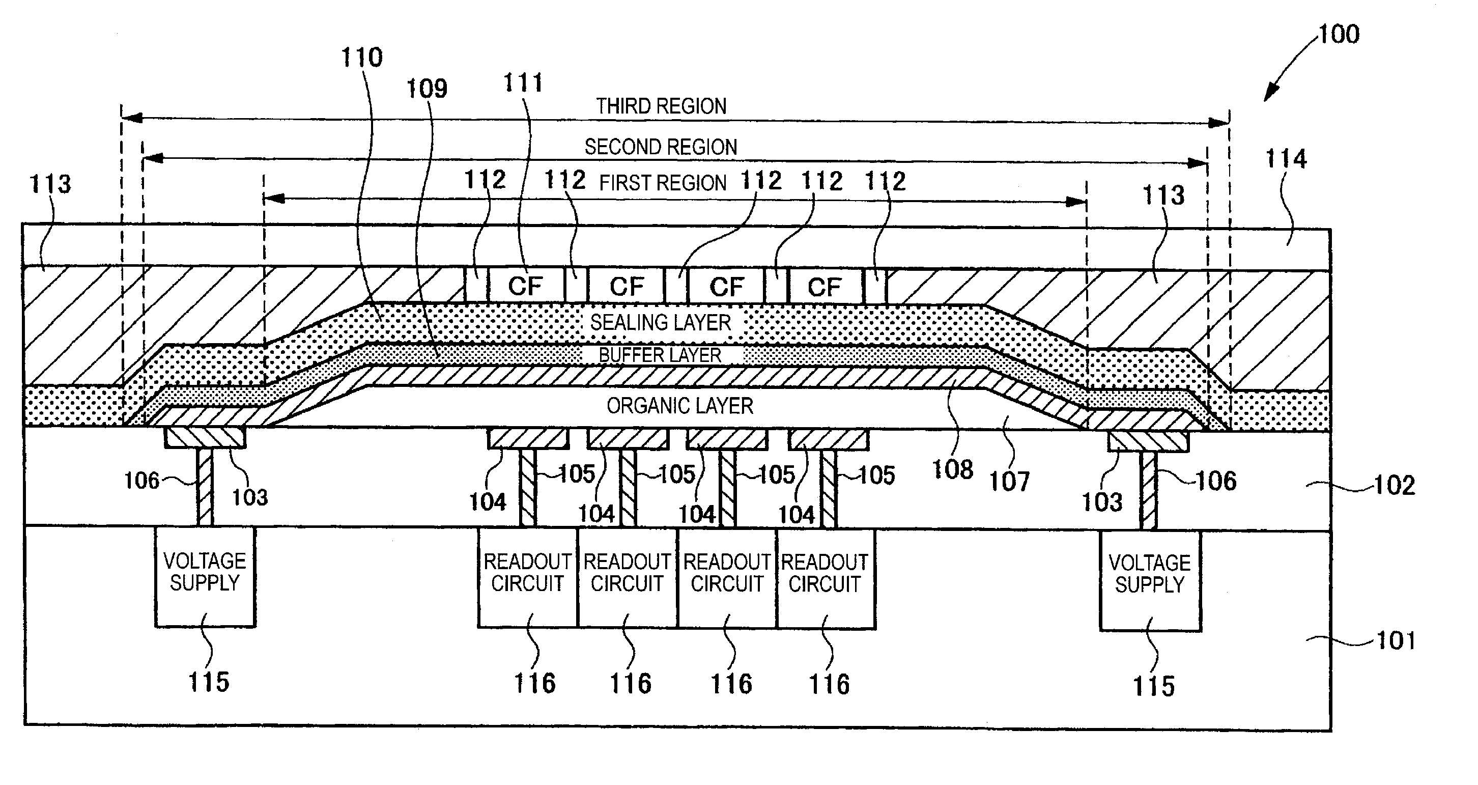
FIELD OF THE INVENTION[0001]This invention relates to a solid-state imaging device, a method of making a solid state imaging device, a digital still camera, a digital video camera, a mobile phone, and an endoscope.BACKGROUND OF THE INVENTION[0002]As image sensors mounted on digital still cameras, digital video cameras, mobile phone cameras, and endoscope cameras, solid state imaging apparatus called CCD sensors or CMOS sensors which include a substrate, e.g., a silicon chip, and an array of pixels containing a photodiode and read out signal charge corresponding to photoelectrons generated in the photodiode of each pixel by a CCD or CMOS readout circuit are known.[0003]The known solid state imaging apparatus includes not only the photodiode but a signal readout circuit and an accompanying multilevel interconnect formed on the semiconductor substrate for every pixel. Therefore, as the pixel pitch reduces, the area ratio of the circuit region in unit pixel becomes larger, which of nece...
Claims
Login to View More Application Information
Patent Timeline
 IPC IPC(8): H01L31/113H01L31/18
CPCH01L27/307H01L51/4273H01L51/448Y02E10/549H04N5/363H04N5/3745H04N9/045H04N5/3532H01L27/14647H04N25/531H04N25/65H04N25/77H04N23/10H04N25/134H10K39/32H10K30/353H10K30/88
InventorNAKATANI, TOSHIHIROGOTO, TAKASHIMAEHARA, YOSHIKISUZUKI, HIDEYUKI
OwnerFUJIFILM CORP