Polarizing film, laminate, and liquid crystal display device
a liquid crystal display device and polarizing film technology, applied in the direction of instruments, organic dyes, polyazo dyes, etc., can solve the problems of reducing the amount of transmitted light in the bright state, destroying the practicability, and destroying the practicability, so as to increase enhance the depolarization effect, and improve the effect of reducing the amount of transmitted ligh
- Summary
- Abstract
- Description
- Claims
- Application Information
AI Technical Summary
Benefits of technology
Problems solved by technology
Method used
Image
Examples
example 1
1. Example 1
(1) Formation of External Polarizing Layer
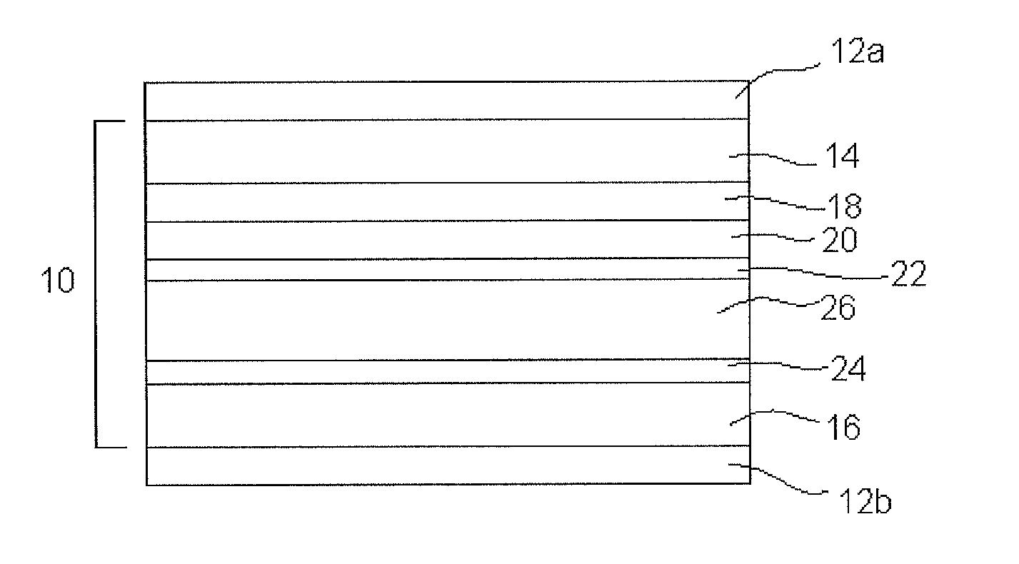
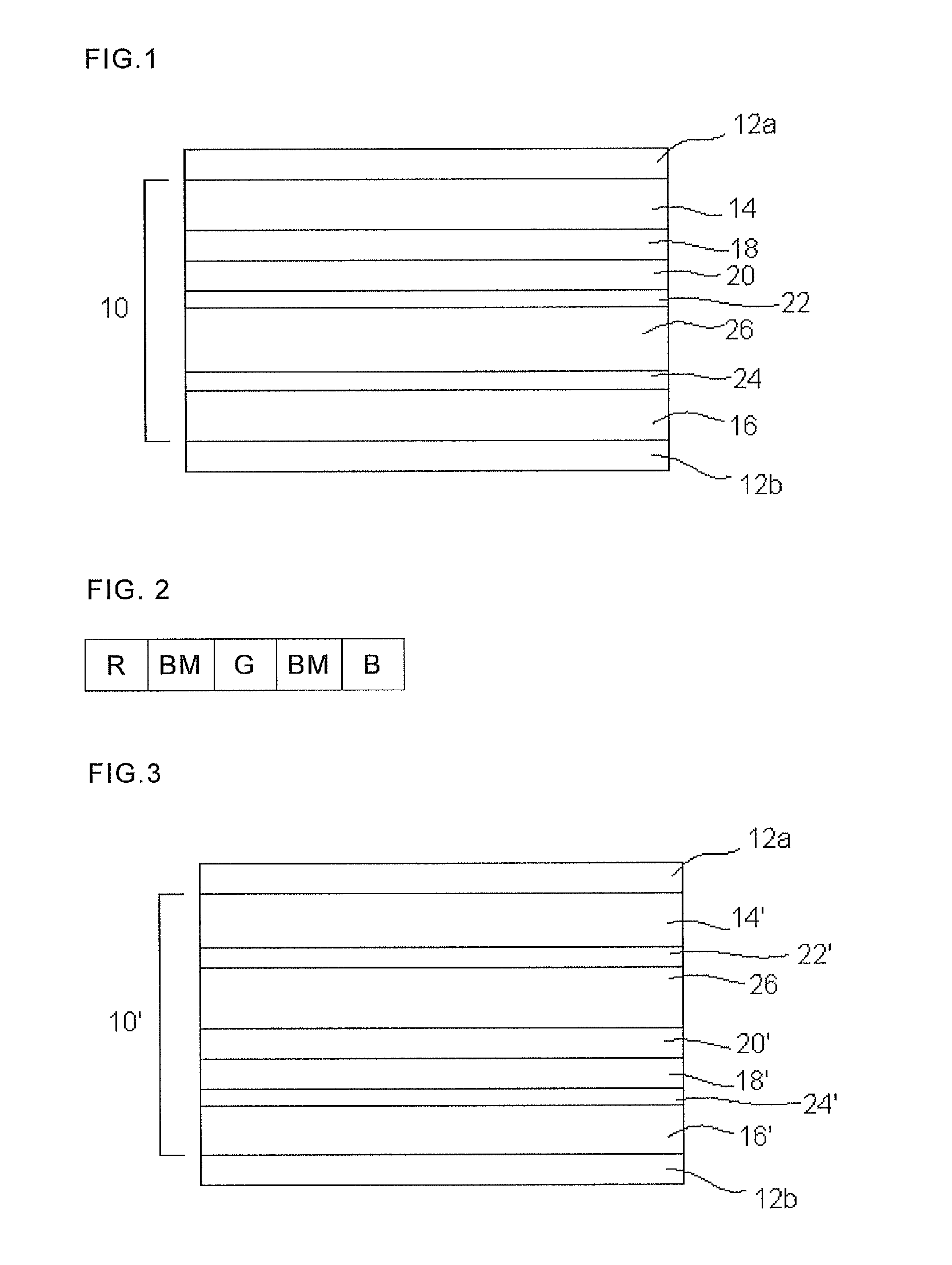
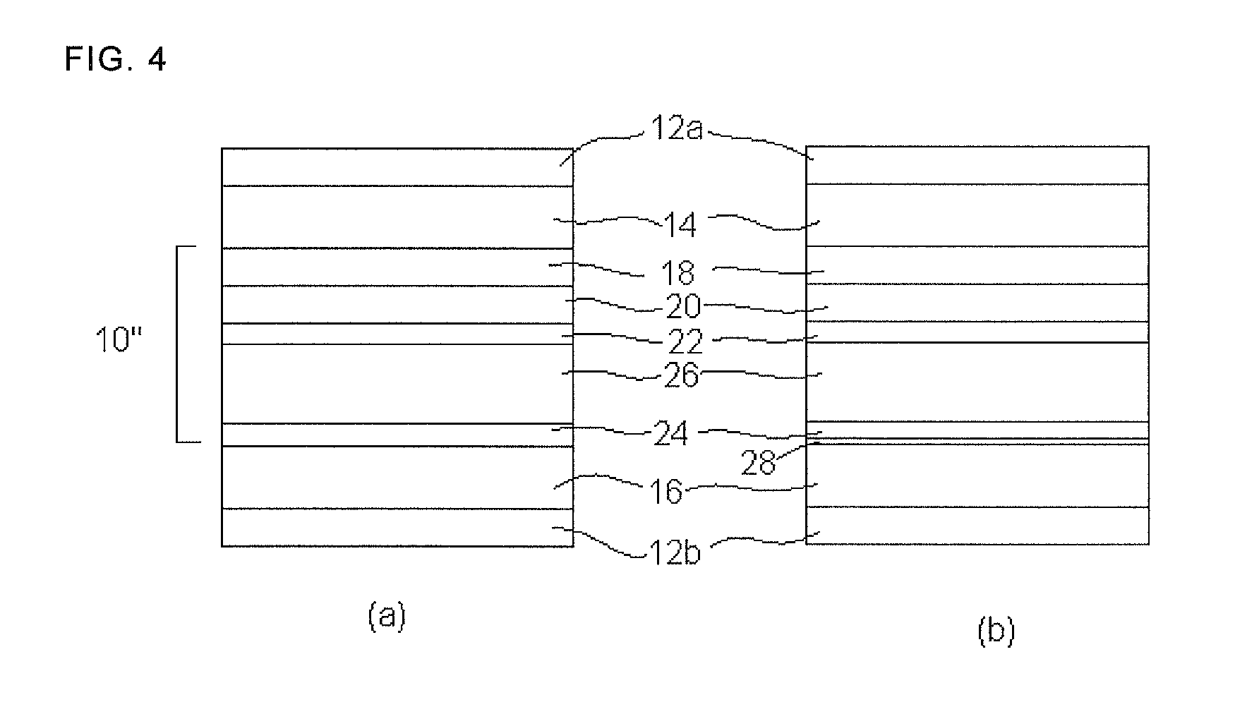
[0205]An iodine-containing polarizing plate was bonded to one surface of a glass plate (liquid crystal cell substrate), while placing an adhesive film in between, to thereby form an external polarizing layer. The degree of polarization of the external polarizing layer, measured by the method described later, was found to be 0.99978, which was nearly equivalent to the degree of polarization of the polarizing plate generally used for the liquid crystal display device.
(2) Formation of Color Filter Layer
[0206]Color resist CG-9500L from FUJIFILM Electronic Materials, Co., Ltd. was coated on the surface of the glass substrate opposite to the surface having the external polarizing layer previously formed thereon, by spin coating at 500 rpm for 20 seconds. The coated film was dried at 80° C. for 5 minutes, and then annealed in an oven at 230° C. for one hour. The color filter layer was thus formed. The depolarization index of the color f...
example 2
2. Example 2
Evaluation of VA Mode Liquid Crystal Display Device
(1) Production of VA Mode Liquid Crystal Display Device C1 of Comparative Example
[0225]A glass substrate of 0.7 mm thick, having a silicon nitride layer which functions as a passivation film preliminarily formed thereon, was obtained, and interconnects such as scanning lines and signal lines, and thin film transistors which function as switching elements were formed on the silicon nitride layer, by repetitive formation and patterning of films, similarly to the general processes of forming film transistors. A ultraviolet-curable transparent resist was then coated thereon, and allowed to cure under ultraviolet irradiation, to thereby form an insulating layer while leaving the throughholes unfilled.
[0226]Next, an ITO film of 200 nm thick was stacked thereon by sputtering, and then etched to form a pixel electrode layer. Over the electrode layer, zigzag-patterned stripes (with a height of 1.5 μm, and a width of the bottom of...
PUM
| Property | Measurement | Unit |
|---|---|---|
| transmittance | aaaaa | aaaaa |
| brightness | aaaaa | aaaaa |
Abstract
Description
Claims
Application Information


