

Mask blank, transfer mask, and methods of manufacturing the same
a technology of mask and mask plate, applied in the field of mask plate, can solve the problems of degradation of line edge roughness (ler) or its optical properties, difficult to ensure sufficient etching, and difficult to use front-surface antireflection layer as etching mask, etc., to achieve the effect of shortening the etching time for cl-based dry etching of the light-shielding layer, enhancing the etching resistance, and improving the etching resistan
- Summary
- Abstract
- Description
- Claims
- Application Information
AI Technical Summary
Benefits of technology
Problems solved by technology
Method used
Image

Examples
example 1
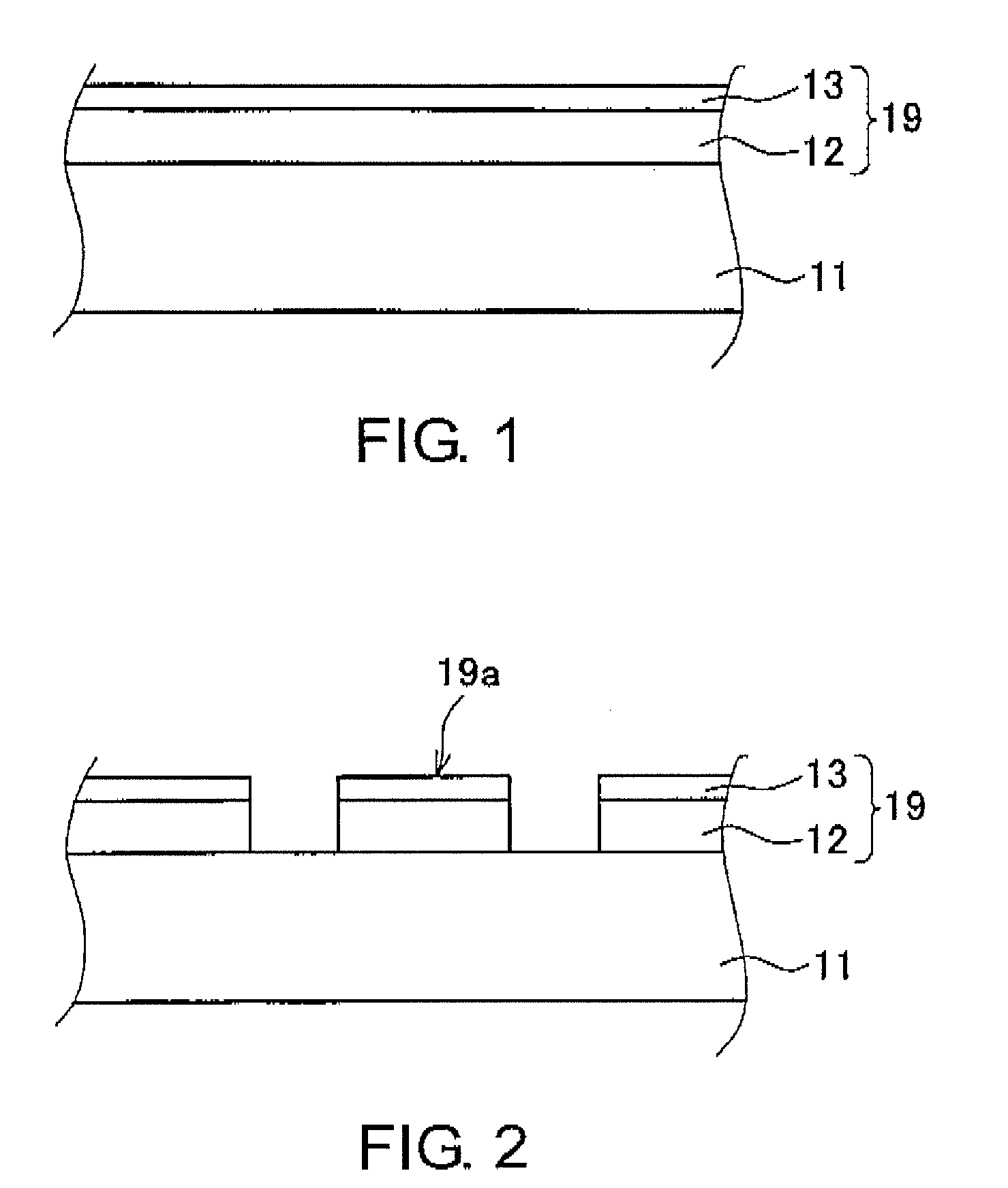
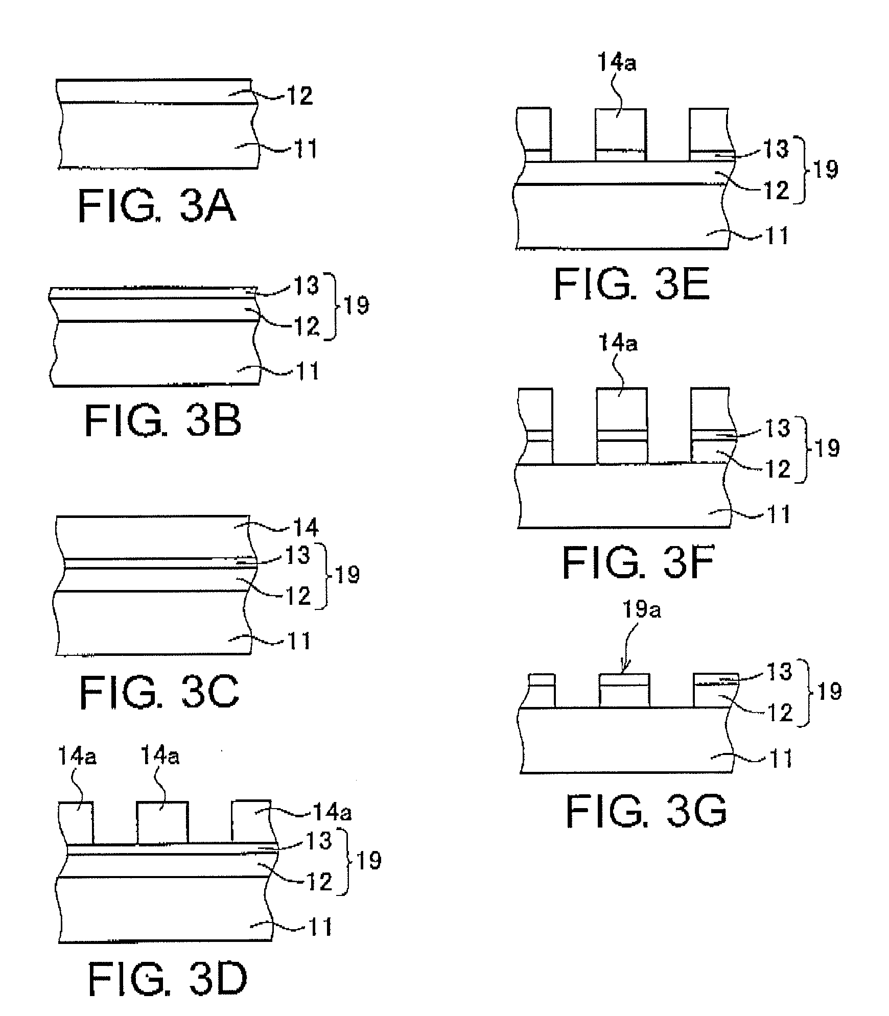
[0085]As shown in FIG. 3A, there was prepared a substrate 11 with precision-polished main surfaces, made of synthetic quartz and having an about 152 mm×152 mm square size with a thickness of about 6.35 mm. Then, the substrate 11 was placed in a single-wafer DC sputtering apparatus. Using a Ta target, a light-shielding layer 12 of TaN (composition ratio Ta: 84.0 at %, N: 16.0 at %) was formed to a thickness of 43 nm by DC magnetron sputtering in a mixed gas atmosphere of xenon (Xe) and nitrogen (N).
[0086]Then, as shown in FIG. 3B, the substrate 11 formed with the light-shielding layer 12 was placed in a single-wafer RF sputtering apparatus where, using a TaSiO mixed sintered target, a front-surface antireflection layer 13 of TaSiO (composition ratio Ta: 27.4 at %, Si: 5.9 at %, O: 66.7 at %) was formed to a thickness of 12 nm on the light-shielding layer 12 by RF magnetron sputtering in an argon (Ar) gas atmosphere. In this manner, an ArF-exposure binary mask blank was manufactured. ...
example 2
[0092]Next, a mask blank according to Example 2 will be described.
[0093]The mask blank according to this Example was manufactured in the same manner as in Example 1 except that a front-surface antireflection layer 13 of a light-shielding film 19 was formed as a TaSiO film (composition ratio Ta: 23.3 at %, Si: 11.7 at %, O: 65 at %) having a thickness of 16 nm. The optical density (OD) of the light-shielding film 19 for the wavelength of ArF excimer laser exposure light was 3.0. Further, with respect to the obtained mask blank, the surface roughness Rq in a 1 μm square area (number of measurement data: 256 points×256 points) on a surface of the light-shielding film 19 was measured by NonoScope III (manufactured by Digital Instrument Corporation). As a result, the surface roughness Rq was 0.32 nm.
[0094]Then, an ArF-exposure binary transfer mask having a light-shielding film pattern 19a was manufactured by the same process as in Example 1. With respect to the obtained transfer mask, th...
example 3
[0096]Next, a mask blank according to Example 3 will be described.
[0097]The mask blank according to this Example was manufactured in the same manner as in Example 1 except that a front-surface antireflection layer 13 of a light-shielding film 19 was formed as a TaSiO film (composition ratio Ta: 30.1 at %, Si: 1.7 at %, O: 68.2 at %) having a thickness of 10 nm. The optical density (OD) of the light-shielding film 19 for the wavelength of ArF excimer laser exposure light was 3.0. Further, with respect to the obtained mask blank, the surface roughness Rq in a 1 μM square area (number of measurement data: 256 points×256 points) on a surface of the light-shielding film 19 was measured by NonoScope III (manufactured by Digital Instrument Corporation). As a result, the surface roughness Rq was 0.34 nm.
[0098]Then, an ArF-exposure binary transfer mask having a light-shielding film pattern 19a was manufactured by the same process as in Example 1. With respect to the obtained transfer mask, t...
PUM
| Property | Measurement | Unit |
|---|---|---|
| thickness | aaaaa | aaaaa |
| thickness | aaaaa | aaaaa |
| thickness | aaaaa | aaaaa |
Abstract
Description
Claims
Application Information