

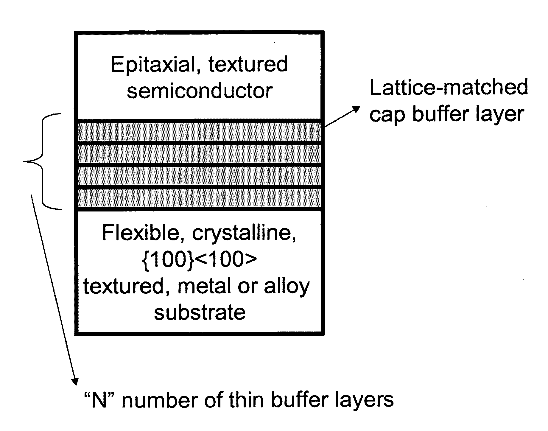
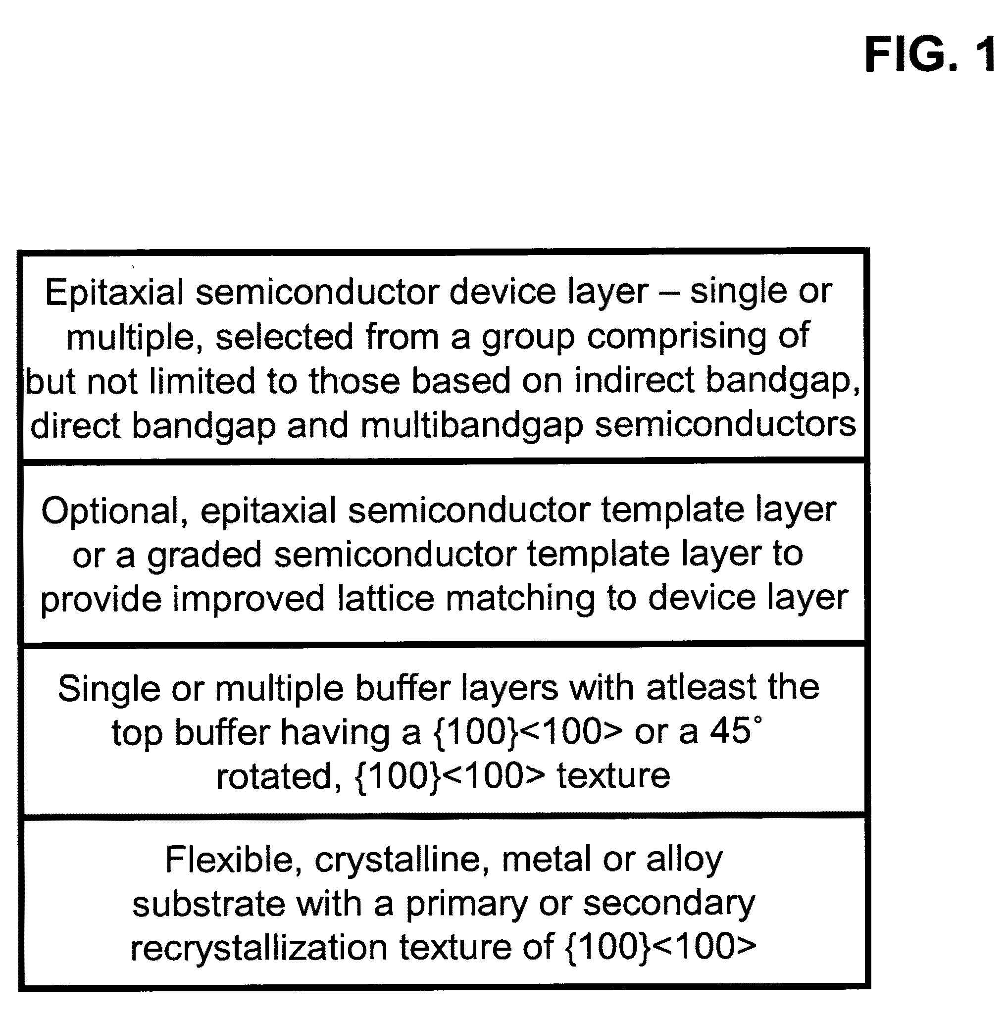
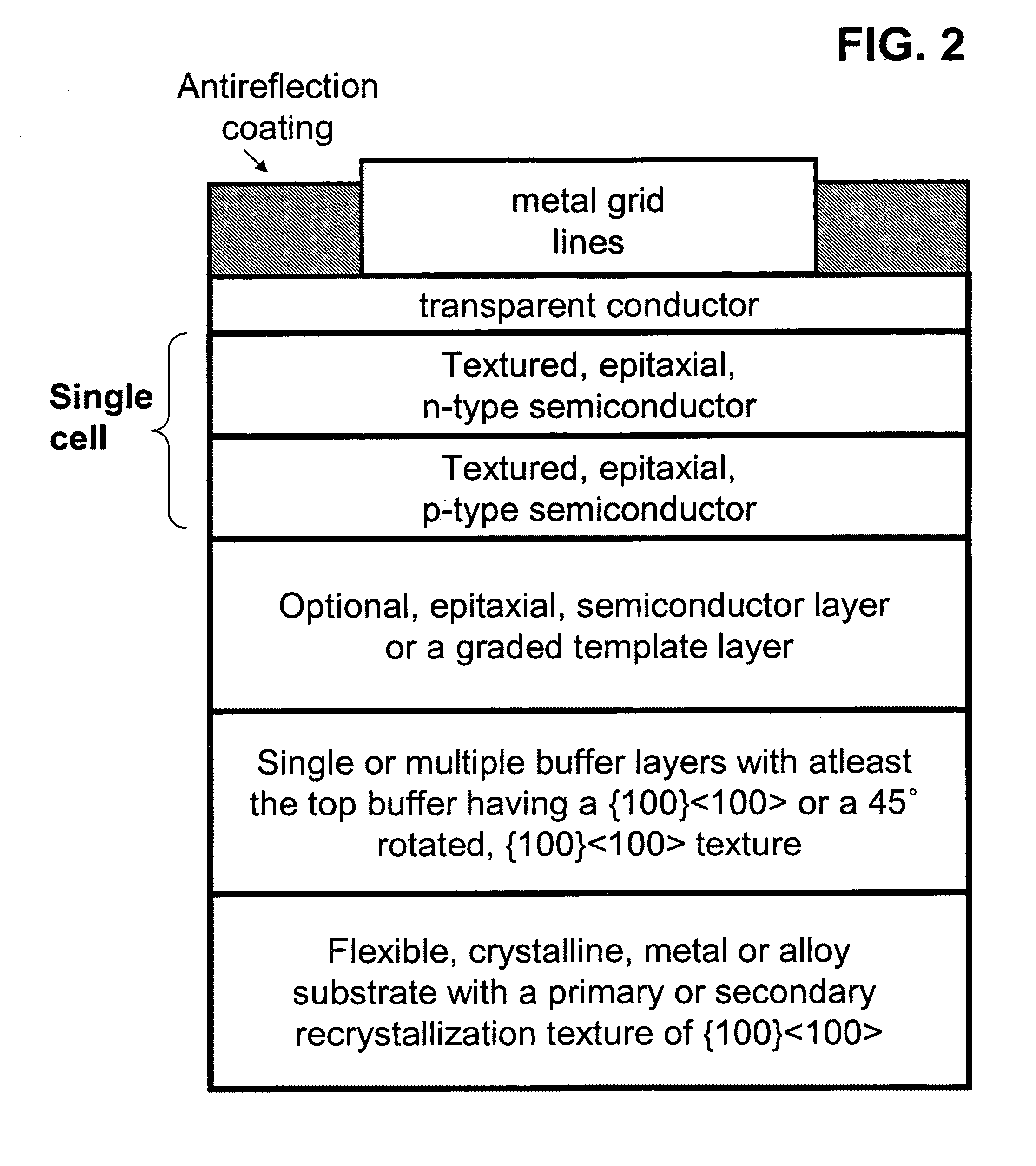
<100> or 45 degrees-rotated <100>, semiconductor-based, large-area, flexible, electronic devices
a technology of electronic devices and rotors, applied in the direction of superconductor devices, semiconductor/solid-state device details, natural mineral layered products, etc., can solve the problems of unrealized solar energy promise, prohibitively expensive cost of single crystal substrates, unfavorable price/performance metric, etc., and achieve good lattice matching
- Summary
- Abstract
- Description
- Claims
- Application Information
AI Technical Summary
Benefits of technology
Problems solved by technology
Method used
Image

Examples
example 1
[0096]A [100], uniaxially textured, metallic substrate was prepared by successively pressing via compression or forging to large total deformations a cubic metal or alloy followed by recrystallization annealing. For example, a NiW alloy with 3-9 at % W was used compressed by 90% deformation in uniaxial compression followed by annealing in a furnace above the primary recrystallization temperature of the alloy. The primary recrystallization texture formed was a [100] texture. By increasing the annealing temperature to high temperatures close to 1000° C., an average grain size larger than 100 μm was formed. Epitaxial buffer layers are then deposited on the substrate. For example, an epitaxial TiN layer was deposited using chemical vapor deposition (CVD) at deposition temperatures in the temperature range of 300-600° C. This is then followed by deposition of an epitaxial Si layer at deposition temperatures in the range of 300-900° C. using a CVD-type process. This results in the formati...
example 2
[0097]A [110], uniaxially textured, metallic substrate was prepared by successively pressing via compression to large total deformations a cubic metal or alloy followed by recrystallization annealing. For example, a NiW alloy with 3-9 at % W was used compressed by 90% deformation in uniaxial compression followed by annealing in a furnace above the primary recrystallization temperature of the alloy. The primary recrystallization texture formed was a [110] texture. By increasing the annealing temperature to high temperatures close to 1000° C., an average grain size larger than 100 μm was formed. Epitaxial buffer layers are then deposited on the substrate. For example, an epitaxial TiN layer was deposited using chemical vapor deposition (CVD) at deposition temperatures in the temperature range of 300-600° C. This is then followed by deposition of an epitaxial Si layer at deposition temperatures in the range of 300-900° C. using a CVD-type process. This results in the formation of a [11...
example 3
[0098]Shown in FIG. 10 is an idealized schematic representation in cross-section of a crystallographically textured, flexible NiW alloy with a textured, epitaxial Si semiconductor layer on top of it with an intervening textured, epitaxial buffer layer of TiN. This device is consistent with the devices depicted in FIGS. 1A and B. [100] textured, biaxially textured Ni-3 at % W was prepared by successive rolling of a powder metallurgy derived alloy coil from about 120 mils to a foil of about 2 mils or 50 microns in thickness. As-rolled crystallographic texture of the foil or tape was the standard Cu-type rolling texture of heavily deformed FCC metals. After the tape was degreased and dried, it was loaded into a reel-to-reel high vacuum (10−8 Torr) chamber, which contained a radio frequency induction heated furnace. The tape was pulled through the hot zone of the furnace at a rate that heated each part to 1250° C. for twenty minutes with a partial pressure of hydrogen sulfide gas of ˜3×...
PUM
| Property | Measurement | Unit |
|---|---|---|
| grain size | aaaaa | aaaaa |
| rotation angle | aaaaa | aaaaa |
| diameter | aaaaa | aaaaa |
Abstract
Description
Claims
Application Information