Radiation detector, method of manufacturing a radiation detector and use of the detector for measuring radiation

a radiation detector and detector technology, applied in the field of radiation detectors, can solve the problems of high cost of silicon detectors, ineffective measurement, and complex cooling, and achieve the effects of high radiation hardness, high counting rate, and fast charge collection

Active Publication Date: 2011-04-07
FINPHYS OY SENCE CENT
View PDF4 Cites 27 Cited by
  • Summary
  • Abstract
  • Description
  • Claims
  • Application Information

AI Technical Summary

Benefits of technology

[0044]There is furthermore preferably a polyethylene moderator at the entrance window for detection of neutrons. The polyethylene is use to slow down the energy of the neutrons then after they will interact with the bohr and generate alpha particles, which will be detected with the detector. Thus, polyethylene is used as a moderator in order to reduce energy. In other words, when the energy of the neutrons is low, they can interact via inelastic nuclear reactions and produce alpha particles. These particles will stop completely in the detector and signals can be detected.
[0049]Moreover, the window passivation layer can have a thickness in the range of only a few nanometers. The columnar structure allows a very fast charge collection, which is essential for high counting rates needed in the case of high intensity particle flow. Finally, the columnar electrodes allow a very high radiation hardness.
[0050]The use of an Silicon On Insulation (SOI) wafer in order to separate the active high resistivity material from the inactive low resistivity material will reduce the effect of charging and polarization after long exposure to heavy ions fluencies.
[0051]The silicon detector of the invention can with stand fluencies of 1015 particles / cm2 without significant degradation of the charge collection efficiency.
[0052]The invention uses a thin silicon wafer in the sensitive volume (a few tens of microns) in order to reduce the sensitivity to background radiation present in plasma. At the same time, the detector will have close to 100% efficiency for detection of ions. The three-dimensional electrode structure is primarily used to avoid the contact layer of the entry window and also to reduce the transit time of the generated charge carriers in the sensitive volume to allow a higher count rate and improve the radiation hardness. With the invention, even count rates in the Megahertz (MHz) scale can be used, compared to the 100 kHz with the detectors of prior art. This will give an increase of the factor of 10-100 times. The capability of the detector is thus improved a lot. The detector of the invention has the best resolution in tracking different charged particles compared to earlier semiconductors and earlier scintillators because of better intrinsic energy resolution and better count rate capability. The resolution compared to the conventional scintillation detectors and semiconductor detectors is expected to be improved with a factor of ten.

Problems solved by technology

The drawback is that silicon detectors are much more expensive than these older technologies and require sophisticated cooling to reduce leakage currents (noise source) as well as suffer degradation over time from radiation.
As a result of the increase in the power of the plasma shots used today for producing ionized particles to be detected, these detectors becomes saturated and consequently made them useless for the measuring and neither is the energy resolution good enough to resolute different ion components.
These detectors can not operate at higher count rates than 100 kHz, mainly due to the CsI(Tl) scintillation time of about 1 microsecond, i.e. they do not allow to carry out pulse high analysis of ion signals under the intensive gamma and neutron background.
Damage cause that the material is not able to work as before and count rate is another problem when the detectors get saturated by the quantity of particles hitting it.
As a consequence of the radiation damage, the energy resolution is worsened and the amplitude of the interested particles become too small that can not be separated from the background signals, which is called degradation of the signal-to-noise ratio.
The reason for the problem arising with is thus that they have a long scintillation time constant, as a consequence of which signals can not be integrated in short time and a low count rate have to be used.
A problem in conventional semiconductor detectors arises when high-intensive radiation such as 1010-1011 neutrons / cm2 is measured because of the intrinsic damage suffers by the silicon bulk of the sensitive volume.
The radiation that hit the detector has time to destroy the detector and induce damages in the sensitive silicon layer, wherein the electrons and holes are intended to be formed.
Also technological problems have set it limitations to the structure of the wafers.
Therefore, such high-intense radiation can not be measured with conventional semiconductor and silicon detectors.
The detection of light ions is very difficult as any material in the input window can reduce the energy, and even stop the incoming ions.
The use of a metal layer in the entrance window is a hinder for detecting ions with low energy and this is due to the thickness of their entrance window.
A second problem with conventional silicon detectors and semiconductor detectors is that when the intention is to measure p (protons), d (deuterons), t (tritons) and a particles, the background radiation containing neutrons and gamma particles should be eliminated.
Conventional semiconductor silicon detectors are not sensitive enough to distinguish between the desired particles and the neutrons and gamma particles since they give more energy to the detected signal than the intended measurements.
When there are intense gamma and neutron backgrounds it is therefore difficult to identify different types of incident particles created in the plasma.

Method used


Image

  • Radiation detector, method of manufacturing a radiation detector and use of the detector for measuring radiation
  • Radiation detector, method of manufacturing a radiation detector and use of the detector for measuring radiation
  • Radiation detector, method of manufacturing a radiation detector and use of the detector for measuring radiation

Examples


Embodiment Construction

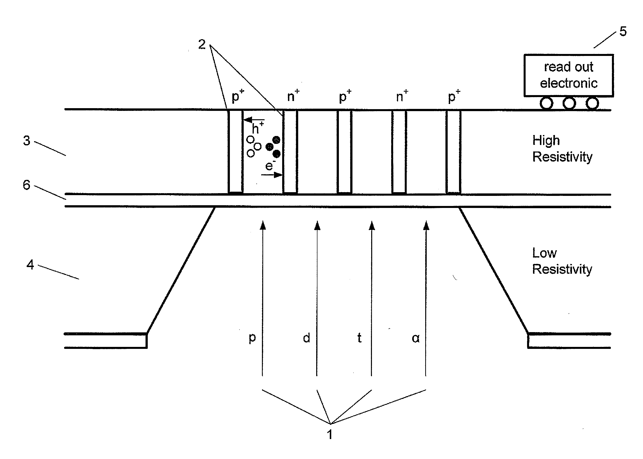
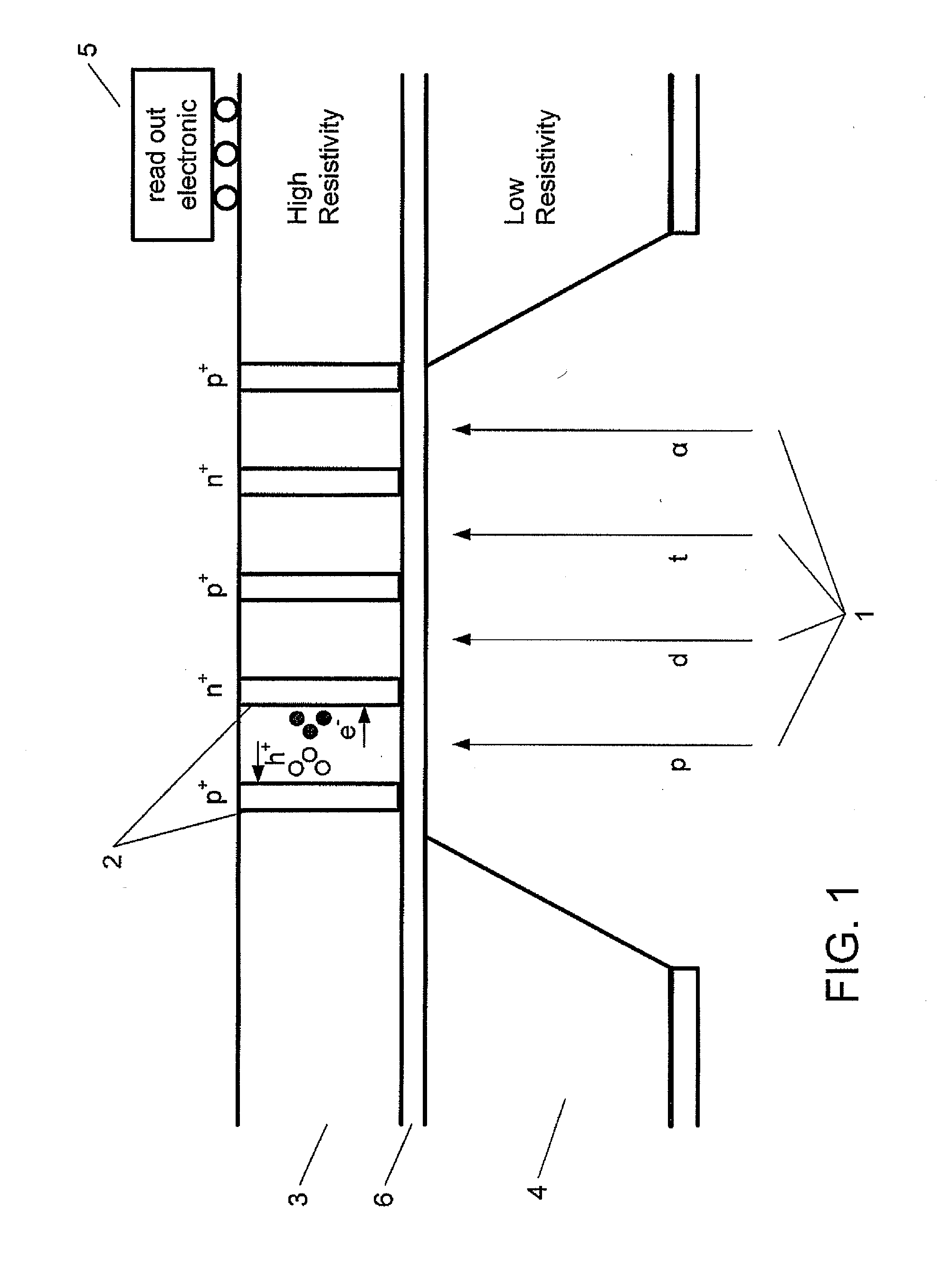
[0060]FIG. 1 is a schematic view of the detector of the invention. The radiation 1 to be detected with the detector of the invention enters the detector as shown in FIG. 1 through an entrance window in a low-resistivity silicon layer 4. The radiation 1 consists of p (protons), d (deuterons), t (tritons) and α particles as well as n (neutrons) and γ particles. It is only the only the α alpha, p protons, d deutrons, and t tritons that are of interest in the invention, the signals generated by the neutrons and gamma particles should be eliminated.

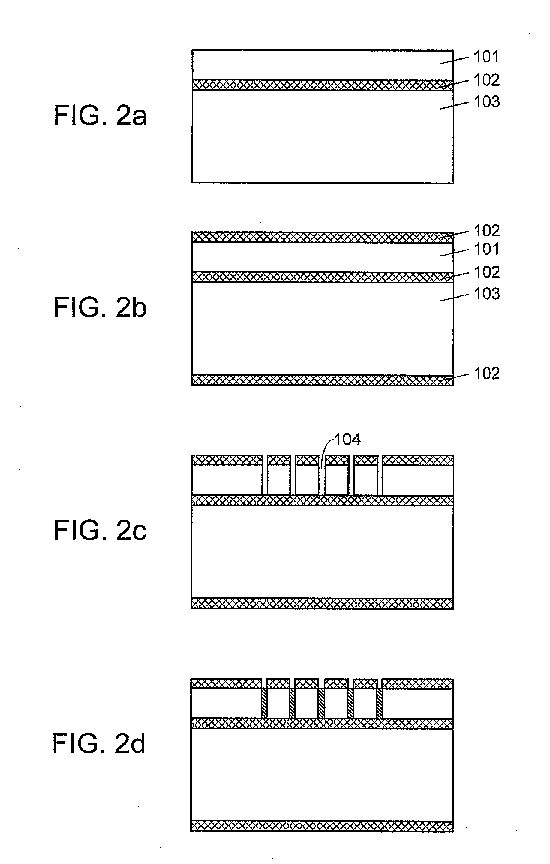
[0061]After having entered the entrance window, the radiation passes the thin passivation layer 6 made of silicon dioxide. This layer is a protective layer that forms a hermetic seal over the circuit elements. This intermediate passivation layer 6 separates the high and low resistivity layers from each other, the thickness being as thin as what is possible from a manufacture view. The function of the passivation is to neutralized the surface c...


PUM


Abstract

A radiation detector is disclosed. The detector has an entrance opening etched through a low-resistivity volume of silicon, a sensitive volume of high-resistivity silicon for converting the radiation particles into detectable charges, and a passivation layer between the low and high-resistivity silicon layers. The detector also has electrodes built in the form of vertical channels for collecting the charges generated in the sensitive volume, and read-out electronics for generating signals based on the collected charges.

Description

CROSS-REFERENCE TO RELATED APPLICATIONS[0001]This application is a continuation of PCT / EP2008 / 066716, filed Dec. 3, 2008, which was published in English and designated the U.S., and claims priority to FI 20070939, filed Dec. 4, 2007, each of which are incorporated herein by reference.BACKGROUND OF THE INVENTION[0002]1. Field of the Invention[0003]The invention is concerned with a silicon detector for detecting high-intensity radiation particles. The silicon detector used comprises a silicon wafer having an entrance opening in low-resistivity silicon, and a passivation layer of silicon dioxide and a sensitive volume of high-resistivity silicon for converting the radiation particles into detectable charges. Furthermore, the detector comprises electrodes built in the form of vertical channels etched into the sensitive volume for collecting the charges, and read-out electronics for generating electrical signals from the collected charges. The invention is also concerned with a method of...

Claims


Application Information

Patent Timeline
Patent Type & Authority Applications(United States)
IPC IPC(8): G01T1/24G01T3/08H01L31/18
CPCH01L27/1446H01L27/14603H01L31/035281H01L27/14683H01L31/035263H01L27/14634G01T1/24G01T3/08H01L31/035272
Inventor GARCIA, FRANCISCOORAVA, RISTOLOZANO, MANUELPELLEGRINI, GIULIO
Owner FINPHYS OY SENCE CENT
Why Eureka
Try Eureka