Process for producing capacitive electromechanical conversion device, and capacitive electromechanical conversion device

a technology of capacitive electromechanical and conversion device, which is applied in the direction of mechanical vibration separation, influence generator, and beacon system using ultrasonic/sonic/infrasonic waves, etc. it can solve the problem of reducing productivity, changing the state of the bonded interface, and difficulty in finer arrangement of elements in an array. the effect of poor bonding at the bonded interface in producing a capacitive electromechanical conversion devi

Inactive Publication Date: 2011-04-14
CANON KK
View PDF17 Cites 68 Cited by
  • Summary
  • Abstract
  • Description
  • Claims
  • Application Information

AI Technical Summary

Benefits of technology

[0023]According to the present invention, poor bonding at the bonded interface in producing a capacitive electromechanical conversion device can be reduced when a cavity is formed between a substrate and a membrane member, because the gas release path is formed and allows the gas, moisture, and the like generated during the production of the element to be released to the outside.

Problems solved by technology

However, the method using annealing requires a few tens to a few hundreds of hours for the annealing step, which may reduce productivity.
On the other hand, the method using a gas-absorbing agent can cause the difficulty in making the elements finer in the arrangement in an array.
In addition, a gas-absorbing agent can cause a change in the state of the bonded interface due to a change associated with absorption.
For this reason, a capacitive electromechanical conversion device requiring a sufficient bonding strength at narrow support portions can cause poor bonding and the like due to the gas generated during the production of the element.

Method used


Image

  • Process for producing capacitive electromechanical conversion device, and capacitive electromechanical conversion device
  • Process for producing capacitive electromechanical conversion device, and capacitive electromechanical conversion device
  • Process for producing capacitive electromechanical conversion device, and capacitive electromechanical conversion device

Examples


example 1

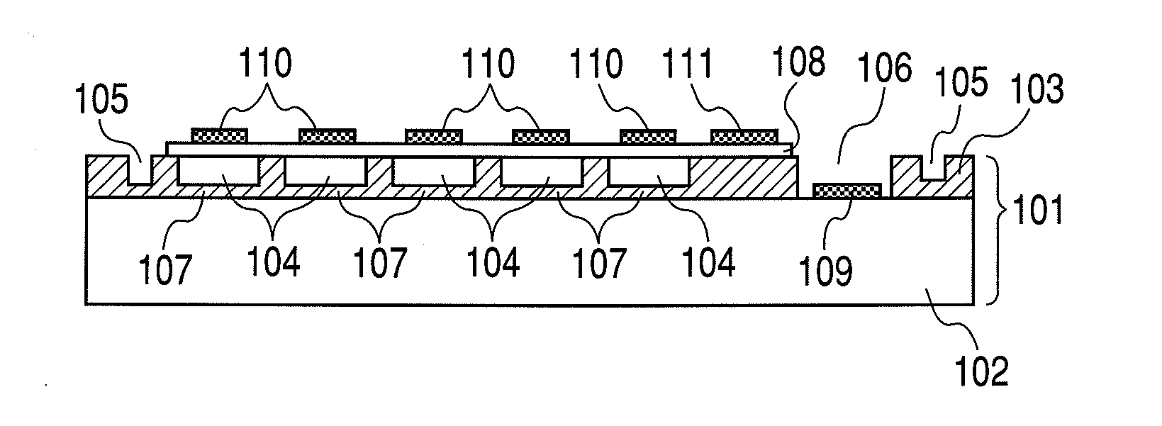
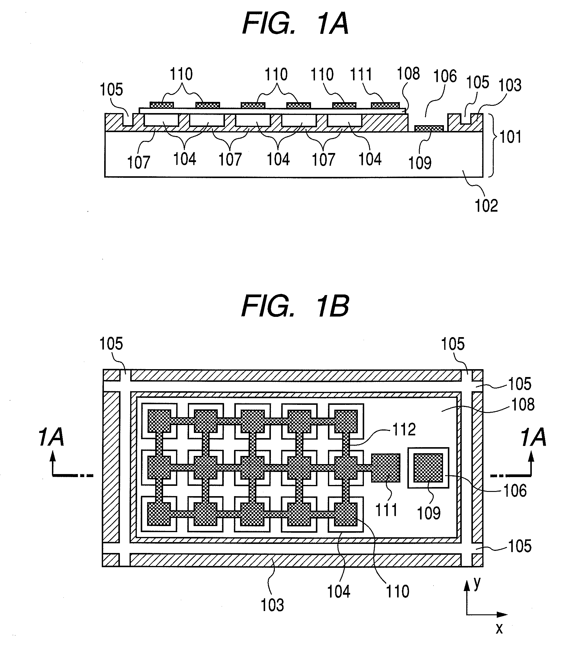
[0046]FIGS. 1A and 1B are a sectional view and a plan view, respectively, illustrating Example 1 relating to the capacitive electromechanical conversion device of the present invention. The same location has the same reference number. The sectional view of FIG. 1A corresponds to the 1A-1A location of FIG. 1B. In the present Example, a substrate 101 includes a silicon single-crystal layer 102, and a silicon oxide film layer 103 formed on the top surface thereof. The silicon single-crystal layer 102 is a substrate for the capacitive electromechanical conversion device, is electrically conductive, and also functions as an electrode. In the silicon oxide film layer 103, cavities (depressed portions) 104, grooves 105 as gas release paths, an electrode extraction portion 106, and electrically insulating layers 107 are formed. In addition, a membrane member 108 is bonded to the silicon oxide film layer 103. The membrane member 108 on the whole is in thin film, the portions formed above the...

example 2

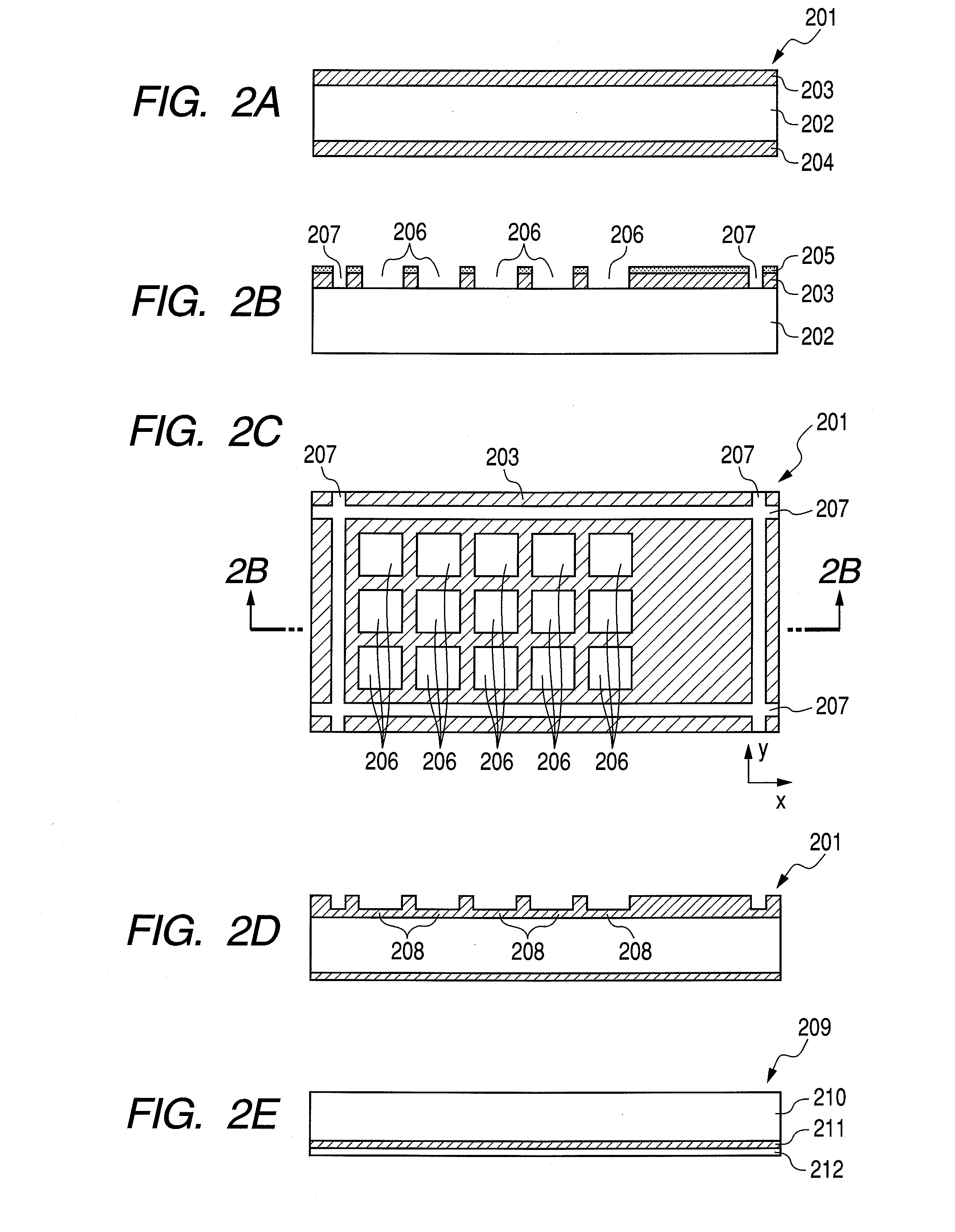
[0063]FIGS. 4A to 4Q are diagrams illustrating Example 2 relating to a process for producing the capacitive electromechanical conversion device of the present invention. The same location has the same reference number. The production process of the present Example begins at a substrate 401, a sectional view of which is illustrated in FIG. 4A. The substrate 401 includes a silicon single-crystal layer 402, and a silicon oxide film layer 403 and a silicon oxide film layer 404 formed on the top and bottom surface thereof, respectively.

[0064]First, as illustrated in FIG. 4B, a photoresist layer 405 is used as an etching resist and a silicon oxide film layer 403 is etched to form cavities (depressed portions) 406. If a hydrofluoric acid is used for etching, a silicon single-crystal layer 402 functions as an etch stop layer, making it easy to control the amount of etching in the depth direction. FIG. 4C illustrates a plan view of the cavities 406 seen from the silicon oxide film layer 403 ...

example 3

[0074]FIGS. 6A to 6H are diagrams illustrating Example 3 relating to a process for producing the capacitive electromechanical conversion device of the present invention. The same location has the same reference number.

[0075]The substrate 401 illustrated in FIG. 6A is the substrate in the same step as in FIG. 4D. In addition, the substrate illustrated in FIG. 6B is an SOI wafer 408, equivalent to that in FIG. 4E, that has a structure where a handle layer 409 comprising a silicon single crystal, a buried oxide film layer 410 comprising silicon oxide, and a device layer 411 comprising a silicon single crystal are laminated together in this order. In the present Example, as illustrated in FIG. 6C, a plurality of pores 601 is formed in the SOI wafer 408 so that the pores penetrate vertically through the wafer. The pores 601 function as gas release pores in a subsequent step. For example, deep reactive ion etching (DRIE) is suitable for processing the pores 601. In DRIE, for example, SF6 ...


PUM

PropertyMeasurementUnit
pressureaaaaaaaaaa
electrical conductivityaaaaaaaaaa
electrically insulatingaaaaaaaaaa

Abstract

A process for producing a capacitive electromechanical conversion device by bonding together a substrate and a membrane member to form a cavity sealed between the substrate and the membrane member, the process for producing a capacitive electromechanical conversion device comprises the steps of: providing a gas release path penetrating from a bonded interface between the substrate and the membrane member to the outside, and forming the cavity by bonding the membrane member with the substrate with the gas release path provided; the gas release path being provided at a location where the path does not communicate with the cavity.

Description

TECHNICAL FIELD[0001]The present invention relates to a process for producing a capacitive electromechanical conversion device such as a transmitting and receiving element used in ultrasonic probes for ultrasonic diagnostic apparatuses, and to a capacitive electromechanical conversion device.BACKGROUND ART[0002]An ultrasonic transducer carries out at least one of the conversion from an electrical signal to ultrasonic and the conversion from ultrasonic to an electrical signal, and is used as a probe for medical imaging and nondestructive testing.[0003]A form of ultrasonic transducer is a capacitive electromechanical conversion device.[0004]U.S. Pat. No. 6,958,255 describes a technology relating to such a capacitive electromechanical conversion device, and FIG. 11 is a sectional view of the basic structure thereof. A silicon single-crystal layer 1101 has electrical conductivity and an electrically insulating layer 1106 is formed on the surface thereof. On the electrically insulating l...

Claims


Application Information

Patent Timeline
Patent Type & Authority Applications(United States)
IPC IPC(8): H02N1/08H05K13/00
CPCB06B1/0292Y10T29/49002G01S1/74
Inventor SOEDA, YASUHIROEZAKI, TAKAHIRO
Owner CANON KK
Why Eureka
Try Eureka