

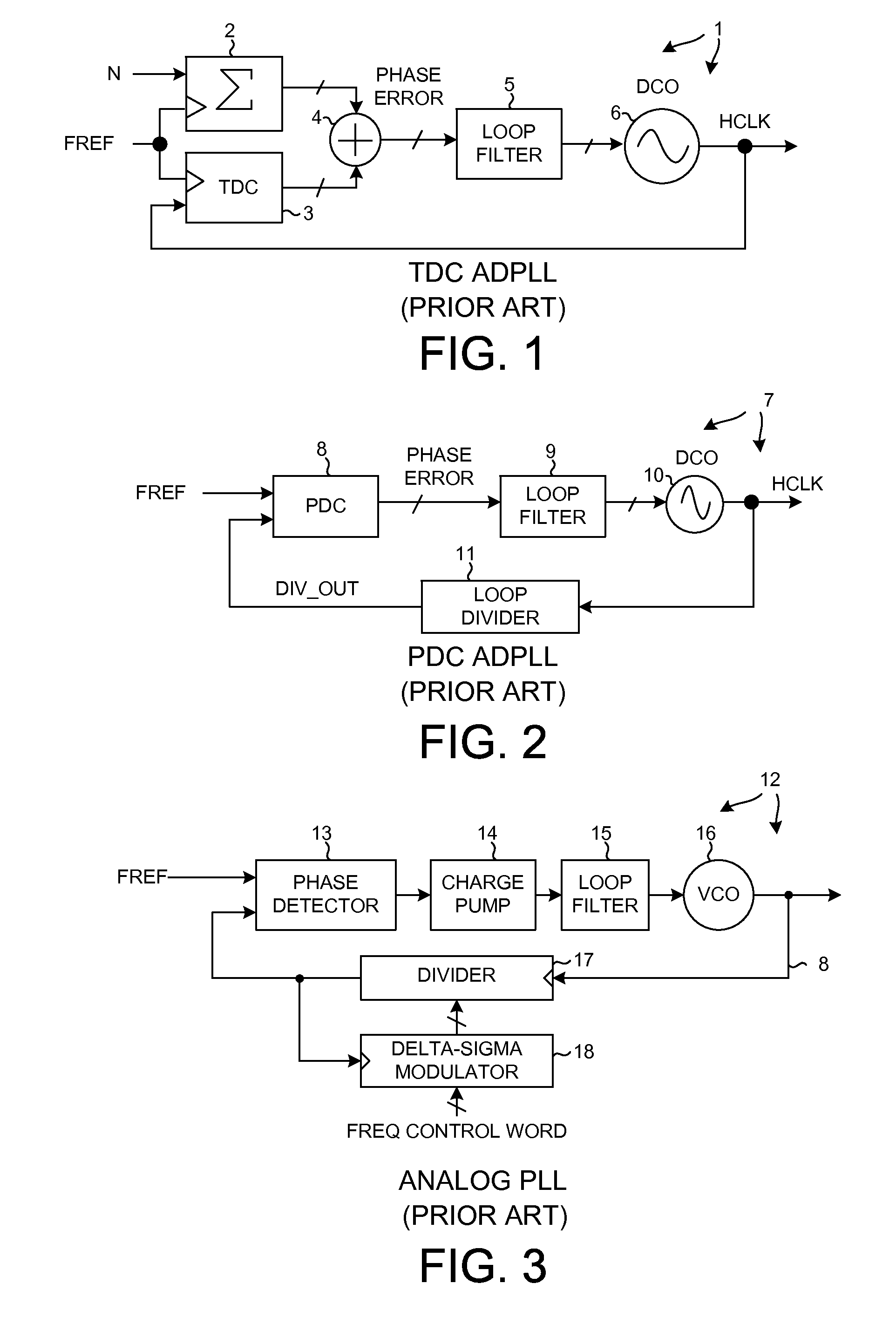
Adc-based mixed-mode digital phase-locked loop
a phase-locked loop and mixed-mode technology, applied in the direction of electric variable regulation, process and machine control, instruments, etc., can solve the problems of complex timing control circuitry, difficult control and calibration of delay lines, and interference by such sources of noise with the proper operation of adpll, so as to reduce power consumption, improve the linearity of charge pumps, and reduce noise of charge pumps
- Summary
- Abstract
- Description
- Claims
- Application Information
AI Technical Summary
Benefits of technology
Problems solved by technology
Method used
Image

Examples
Embodiment Construction
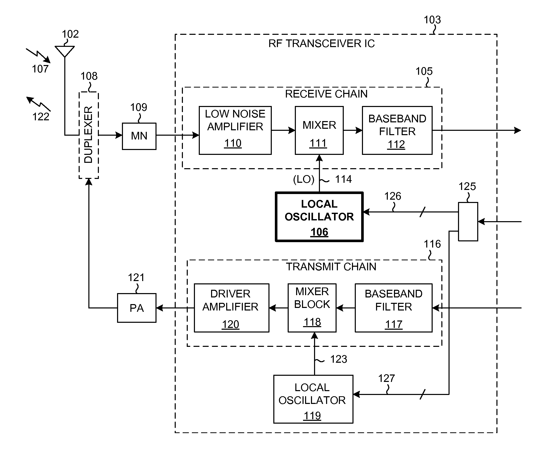
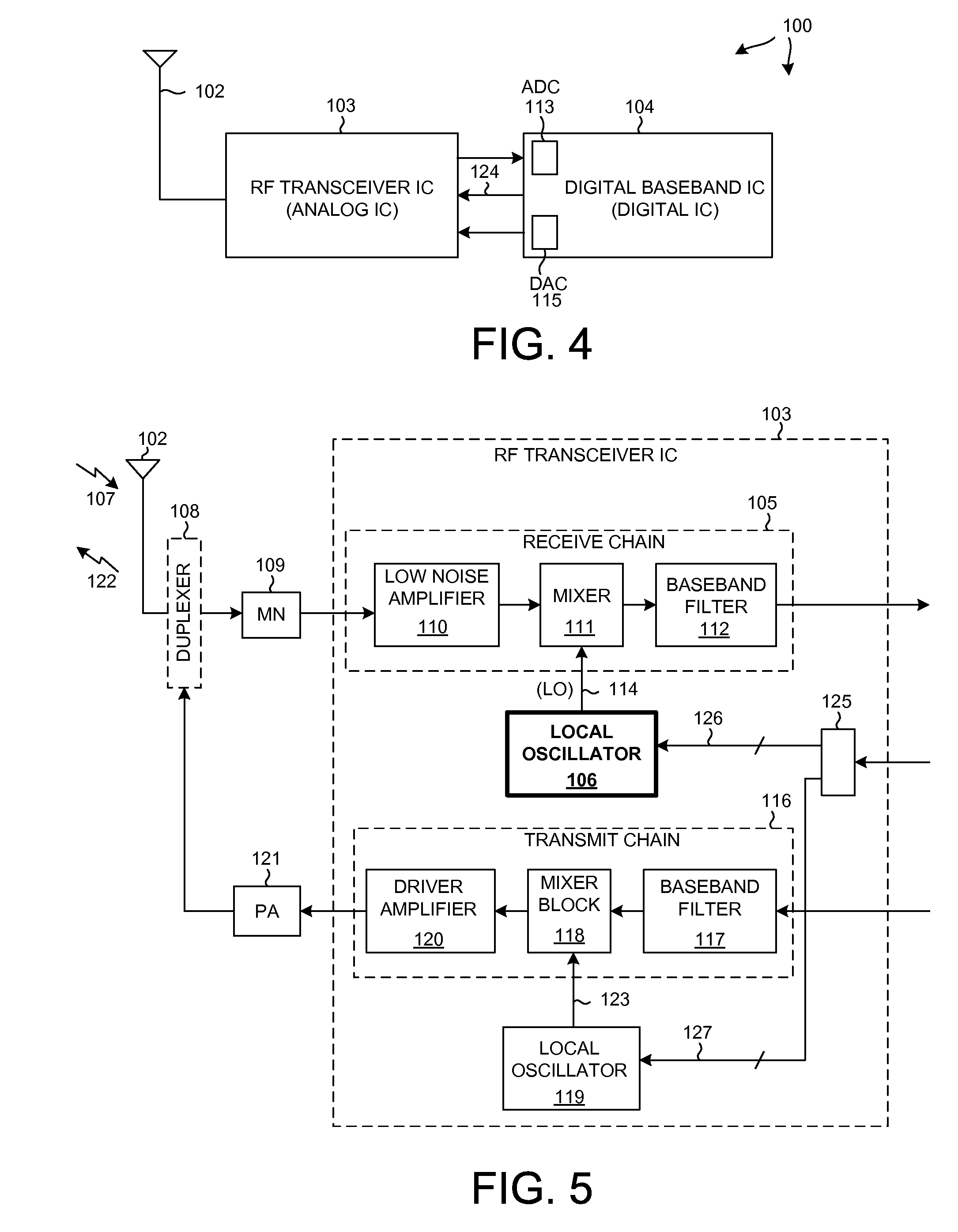
[0029]FIG. 4 is a very simplified high level block diagram of one particular type of mobile communication device 100 in accordance with one novel aspect. In this example, mobile communication device 100 is a cellular telephone that uses a Code Division Multiple Access (CDMA) cellular telephone communication protocol. The cellular telephone includes (among several other parts not illustrated) an antenna 102 and two integrated circuits 103 and 104. Integrated circuit 104 is called a “digital baseband integrated circuit” or a “baseband processor integrated circuit”. Integrated circuit 103 is an RF transceiver integrated circuit. RF transceiver integrated circuit 103 is called a “transceiver” because it includes a transmitter as well as a receiver.
[0030]FIG. 5 is a more detailed block diagram of the RF transceiver integrated circuit 103 of FIG. 4. The receiver includes what is called a “receive chain”105 as well as a Local Oscillator (LO) 106. When the cellular telephone is receiving, a...
PUM
 Abstract
Description
Claims
Application Information