Group-iii nitride semiconductor light-emitting device, method for manufacturing the same, and lamp

a nitride semiconductor and light-emitting device technology, applied in semiconductor devices, electrical devices, nanotechnology, etc., can solve the problems of difficult epitaxial growth of crystals directly on the substrate, inability to improve the crystallinity of the entire wafer surface, and inability to epitaxially grow crystals on the substrate, etc., to achieve high-level light emission output, improve internal quantum efficiency, and superimpose crystallinity

Active Publication Date: 2011-04-28
TOYODA GOSEI CO LTD
View PDF5 Cites 32 Cited by
  • Summary
  • Abstract
  • Description
  • Claims
  • Application Information

AI Technical Summary

Benefits of technology

[0070]According to the group-III nitride semiconductor light-emitting device of the present invention, there is provided a configuration such that an AlN seed layer composed of a group-III nitride based compound is laminated on a substrate, and on this AlN seed layer, there are sequentially laminated each layer of an n-type semiconductor layer, a light-emitting layer, and a p-type semiconductor layer respectively composed of a group-III nitride semiconductor, in which the full width at half-maximum of the rocking curve in the (0002) plane of the p-type semiconductor layer is 60 arcse

Problems solved by technology

However, between such different types of substrates and group-III nitride semiconductor crystals epitaxially grown thereon, there is a considerable lattice misfit.
In general, if such a considerable lattice misfit is present as described above, it becomes difficult to epitaxially grow crystals directly on the substrate.
However, while this method partially improves crystallinity, it does not improve crystallinity of the entire wafer surface.
Therefore, application of this method has not been preferred for an LED, in which cost is an important factor and the number of devices obtained from a single wafer is important, while the method may be applied to a laser diode.
In these cases of Non-Patent Documents 1 and 2, the above problem occurs even if the dis

Method used


Image

  • Group-iii nitride semiconductor light-emitting device, method for manufacturing the same, and lamp
  • Group-iii nitride semiconductor light-emitting device, method for manufacturing the same, and lamp
  • Group-iii nitride semiconductor light-emitting device, method for manufacturing the same, and lamp

Examples


experimental example 1

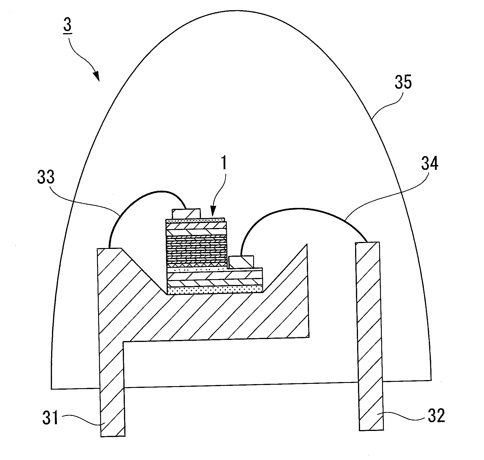
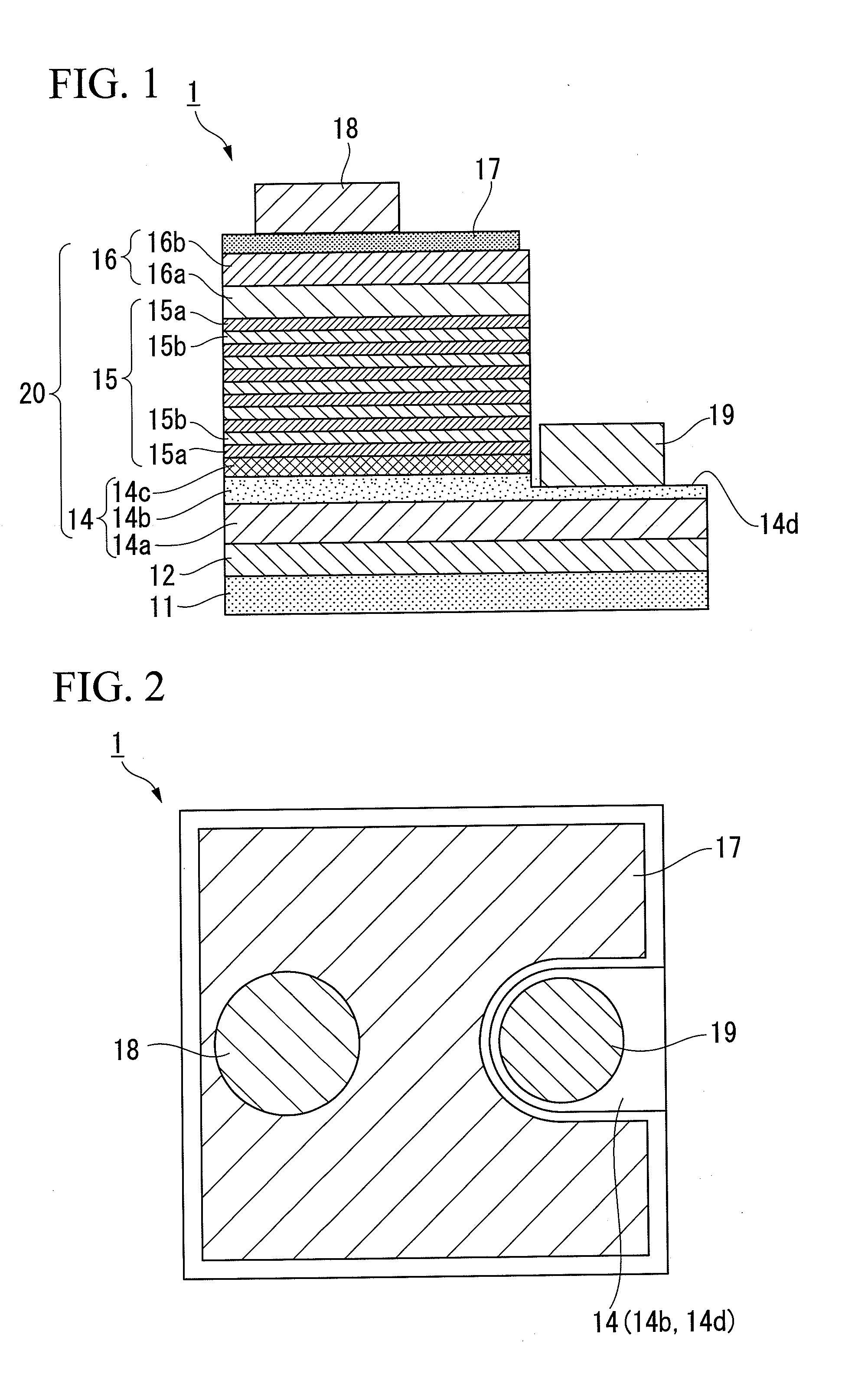
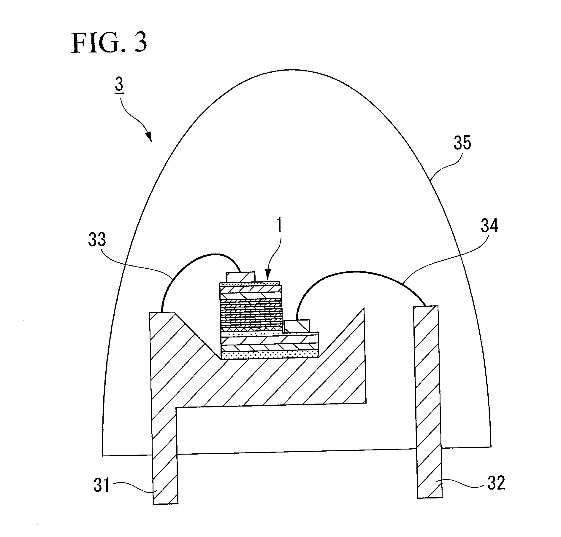
[0250]FIG. 1 shows a cross-sectional schematic view of the laminated semiconductor of the group-III nitride semiconductor light-emitting device manufactured in the present example. In the present experimental example, on the c-plane of a sapphire substrate, there was formed, a layer composed of AlN which serves as an AlN seed layer, and on this, there was formed, by means of an MOCVD method, a layer composed of GaN which serves as a base layer.

[0251]First, there were prepared 100 substrates formed from C-plane sapphire with 100 mm diameter and 0.9 mm thickness, which were all obtained through the same processing steps. This substrate was cut out with OFF angle 0.35°, and the surface thereof was Ra≦2 Å.

[0252]Next, this substrate underwent wet cleaning in which the substrate was rotated at 500 rpm and purified water was injected thereat, and then, the substrate rotation speed was increased to 2,000 rpm and a drying treatment was conducted.

[0253]Subsequently, the substrate was introduc...

experimental examples 2 to 11

[0288]With the exception that at the time of forming the light-emitting layer, the thickness of the barrier layer was respectively changed to the thickness shown in Table 4 by changing the time for growing the barrier layer which constitutes a multiple quantum well structure, LED chip samples of Experimental Examples 2 to 11 were manufactured in a procedure similar to that of Experimental Example 1 above. As with Experimental Example 1, a list of measurement results of the electrical characteristics and light emission characteristics, and a list of measurement results of FWHM of the AlN seed layer and the p-type semiconductor layer are shown in Table 4.

experimental examples 12 to 15

[0289]The conditions of substrate cleaning and the film formation conditions of AlN were set as shown in Table 1, in a procedure similar to that of Experimental Example 1 above, an AlN seed layer was laminated on a substrate, and respective layers were laminated thereon, to thereby manufacture LED chip samples of Experimental Examples 12 to 15. As with Experimental Example 1, a list of measurement results of the electrical characteristics and light emission characteristics, and a list of measurement results of FWHM of the AlN seed layer and the p-type semiconductor layer are shown in Table 3.

[Evaluation Results of Respective Experimental Examples]

[0290]As shown in Table 4, it can be understood that the samples of Experimental Examples 1 to 4, in which the total film thickness of the thickness of the single barrier layer constituting the light-emitting layer, and the thickness of the adjacent well layer, was in an appropriate range, had a high level of crystallinity in the p-type sem...


PUM


Abstract

Provided is a group-III nitride semiconductor light-emitting device which has a high level of crystallinity and superior internal quantum efficiency and which is capable of enabling acquisition of high level light emission output, and a manufacturing method thereof, and a lamp. An AlN seed layer composed of a group-III nitride based compound is laminated on a substrate 11, and on this AlN seed layer, there are sequentially laminated each layer of an n-type semiconductor layer, a light-emitting layer, and a p-type semiconductor layer respectively composed of a group-III nitride semiconductor, wherein the full width at half-maximum of the X-ray rocking curve of the (0002) plane of the p-type semiconductor layer 16 is 60 arcsec or less, and the full width at half-maximum of the X-ray rocking curve of the (10-10) plane is 250 arcsec or less.

Description

FIELD OF THE INVENTION[0001]The present invention relates to a group-III nitride semiconductor light-emitting device suitably used for a light-emitting diode (LED), a laser diode (LD), an electronic device, and the like, a method for manufacturing the same, and a lamp which uses a group-III nitride based compound semiconductor light-emitting device.[0002]Priority is claimed on Japanese Patent Application No. 2008-159690, filed Jun. 18, 2008, the contents of which are incorporated herein by reference.BACKGROUND ART[0003]A group-III nitride based compound semiconductor is a direct transition type semiconductor, which is used as a light-emitting device, for example, has a wide range light-emission spectrum covering ultraviolet to red, and it is applied to light-emitting devices such as a light-emitting diode (LED) and laser diode (LD). This type of light-emitting device has a higher light emission efficiency compared to a conventional illumination-related light source, and therefore a ...

Claims


Application Information

Patent Timeline
IPC IPC(8): H01L33/32B82Y10/00B82Y20/00B82Y40/00H01L21/205H01L33/06H01L33/56H01L33/62
CPCH01L21/02378H01L21/0242H01L2924/3025H01L2224/73265H01L2224/49107H01L2224/48257H01L2224/48247H01L2224/48091H01L2224/32245H01L2224/45144H01L33/32H01L33/16H01L33/12H01L21/0262H01L21/02579H01L21/02433H01L21/02458H01L21/0254H01L2924/00014H01L2924/00H01L2924/181H01L2924/00012
Inventor HANAWA, KENZOSAKAI, HIROMITSUSASAKI, YASUMASA
Owner TOYODA GOSEI CO LTD
Why Eureka
Try Eureka