

Semiconductor device
a technology of semiconductor devices and dielectric devices, which is applied in the direction of solid-state devices, basic electric elements, capacitors, etc., can solve the problems of shortening the traveling distance of leakage current of in-vehicle electronic devices, increasing the power consumption of semiconductor devices, and limited use time, so as to reduce hydrogen concentration and suppress the generation of parasitic channels , the effect of reducing the amount of hydrogen concentration
- Summary
- Abstract
- Description
- Claims
- Application Information
AI Technical Summary
Benefits of technology
Problems solved by technology
Method used
Image

Examples
embodiment 1
[0052]In Embodiment 1, an example of a cross-sectional structure of a semiconductor integrated circuit will be described.
[0053]One embodiments of a semiconductor integrated circuit of the present invention and a manufacturing method thereof will be described with reference to FIGS. 1A and 1B, FIG. 2, FIG. 3, and FIGS. 4A and 4B.
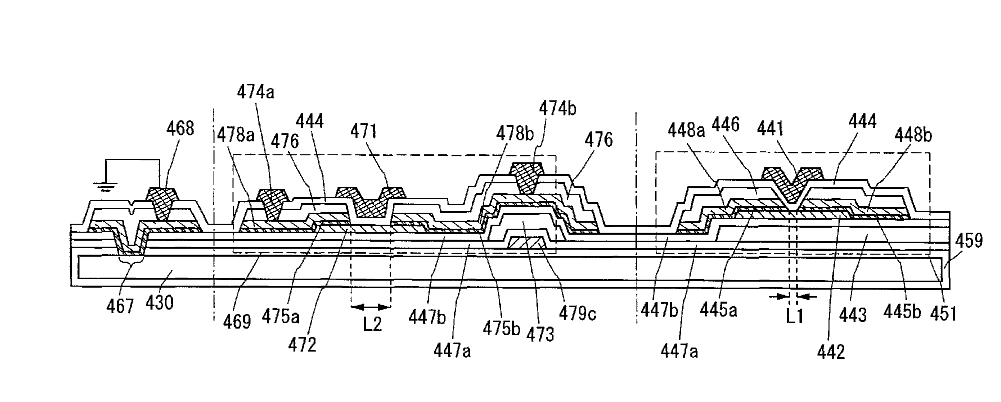
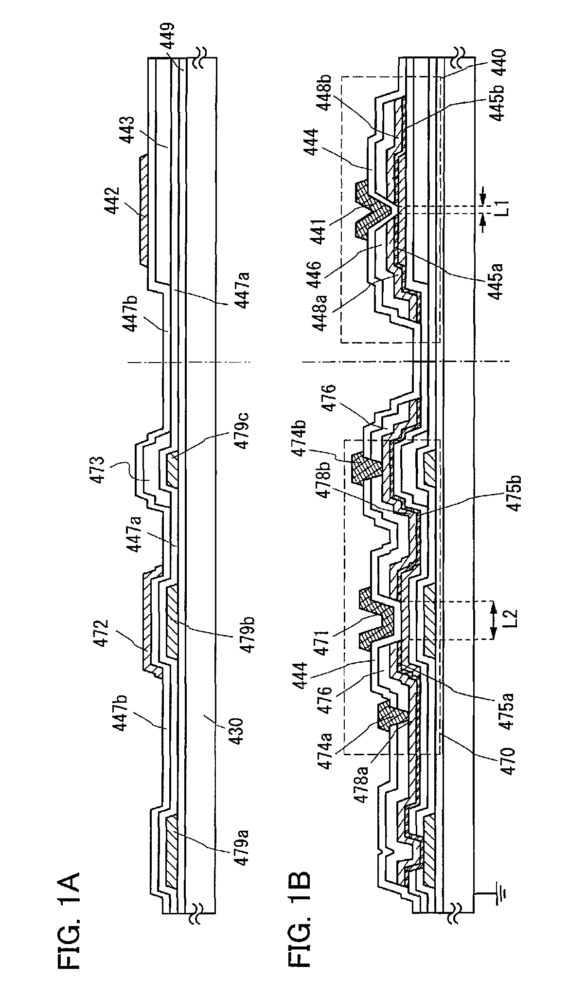
[0054]FIGS. 1A and 1B illustrate an example of a cross-sectional structure of a semiconductor device. A transistor 440 illustrated in FIG. 1B is a top-gate transistor.
[0055]The transistor 440 includes over a semiconductor substrate 430, an insulating film 449, a first insulating layer 447a, a second insulating layer 443, a third insulating layer 447b, an oxide semiconductor layer 442, a first source electrode layer 445a, a second source electrode layer 448a, a first drain electrode layer 445b, a second drain electrode layer 448b, a fourth insulating layer 446, a gate insulating layer 444, and a gate electrode layer 441.
[0056]Part of the oxide semiconductor la...
embodiment 2
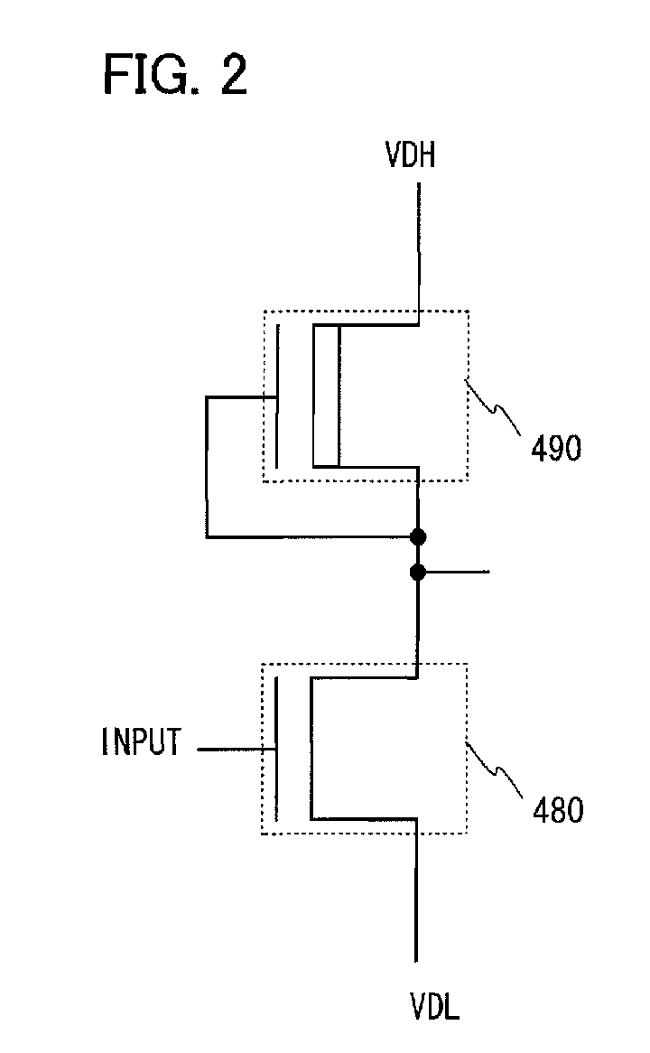
[0136]In Embodiment 2, an example of forming an inverter circuit of an integrated circuit with the use of two n-channel transistors will be described. The manufacturing process of the transistor is almost the same as that in Embodiment 1, and therefore, only a difference is described in detail.
[0137]The integrated circuit is formed using an inverter circuit, a capacitor, a resistor, and the like; therefore, a process of forming a capacitor and two kinds of resistors over the same substrate in addition to the inverter circuit is also described.
[0138]When the inverter circuit is formed using two n-channel TFTs in combination, there are the following cases: an EDMOS circuit having a combination of an enhancement type transistor and a depletion type transistor; and an inverter circuit having a combination of two enhancement type TFTs (hereinafter, referred to as an EEMOS circuit).
[0139]In Embodiment 2, an example of the EDMOS circuit is described. An equivalent circuit of the EDMOS circ...
embodiment 3
[0161]In Embodiment 3, an example of manufacturing a CPU (central processing unit) with the use of the EDMOS circuit described in Embodiment 2 will be described.
[0162]An example of a block diagram of a CPU is illustrated in FIG. 5. A CPU 1001 illustrated in FIG. 5 includes a timing control 1002, an instruction decoder 1003, a register array 1004, an address logic and buffer 1005, a data bus interface 1006, an ALU 1007, an instruction register 1008, and the like.
[0163]These circuits are manufactured using the transistor, the inverter circuit, the resistor, the capacitor, and the like described in Embodiment 1 or Embodiment 2. Since the transistor described in Embodiment 1 or 2 is formed over a semiconductor substrate and includes an oxide semiconductor layer with sufficiently reduced hydrogen concentration, the off-current of the transistor can be reduced to be extremely small value. Therefore, at least part of the CPU 1001 is formed using the transistor which is formed over a semico...
PUM
 Abstract
Description
Claims
Application Information