
Ferroelectric organic memories with ultra-low voltage operation

a technology of organic memories and ferroelectric devices, which is applied in the field of memory devices and recording media, can solve the problems of deterioration of ferroelectric properties, long switching time under a given voltage, and degradation of the interface between the electrodes, and achieve good ferroelectric switching performan

Inactive Publication Date: 2011-05-12
UNIVERSITE CATHOLIQUE DE LOUVAIN
View PDF15 Cites 13 Cited by
  • Summary
  • Abstract
  • Description
  • Claims
  • Application Information

AI Technical Summary

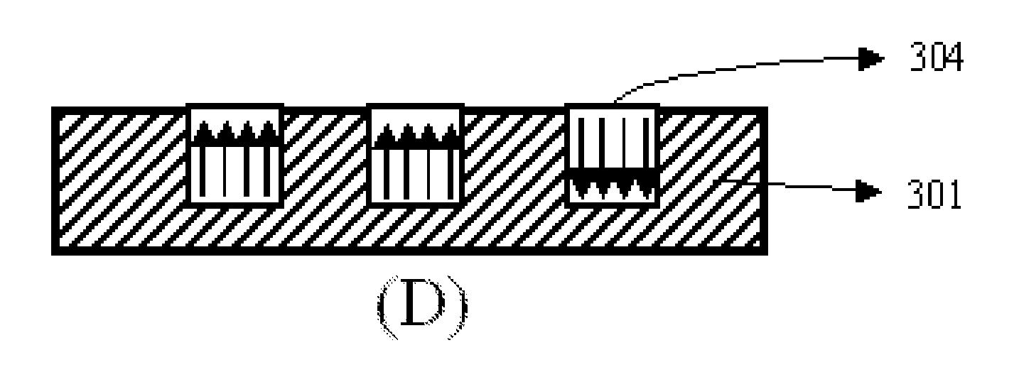
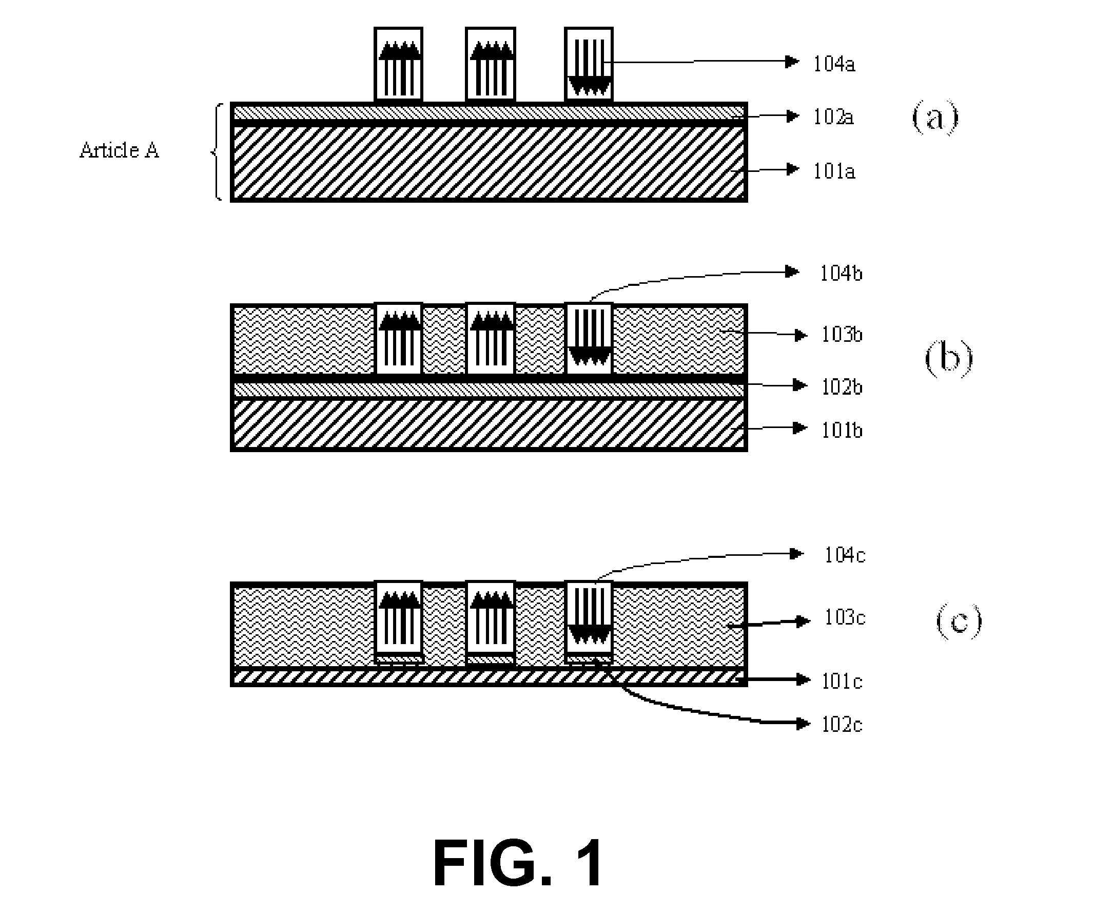
Benefits of technology

[0010]It is an object of the present invention to provide methods to manufacture ferroelectric organic memory devices with good ferroelectric switching performances.
[0011]It is an advantage of embodiments of the present invention that a low operation voltage in ferroelectric organic memory devices can be achieved. It is also an advantage of embodiments of the present invention that fast switching speed in ferroelectric organic memory devices can be achieved. It is also an advantage of embodiments of the present invention that a high signal-to-noise ratio in the data reading process of ferroelectric organic memory devices can be achieved. It is also an advantage of embodiments of the present invention that high storage density in ferroelectric organic memory devices can be achieved.
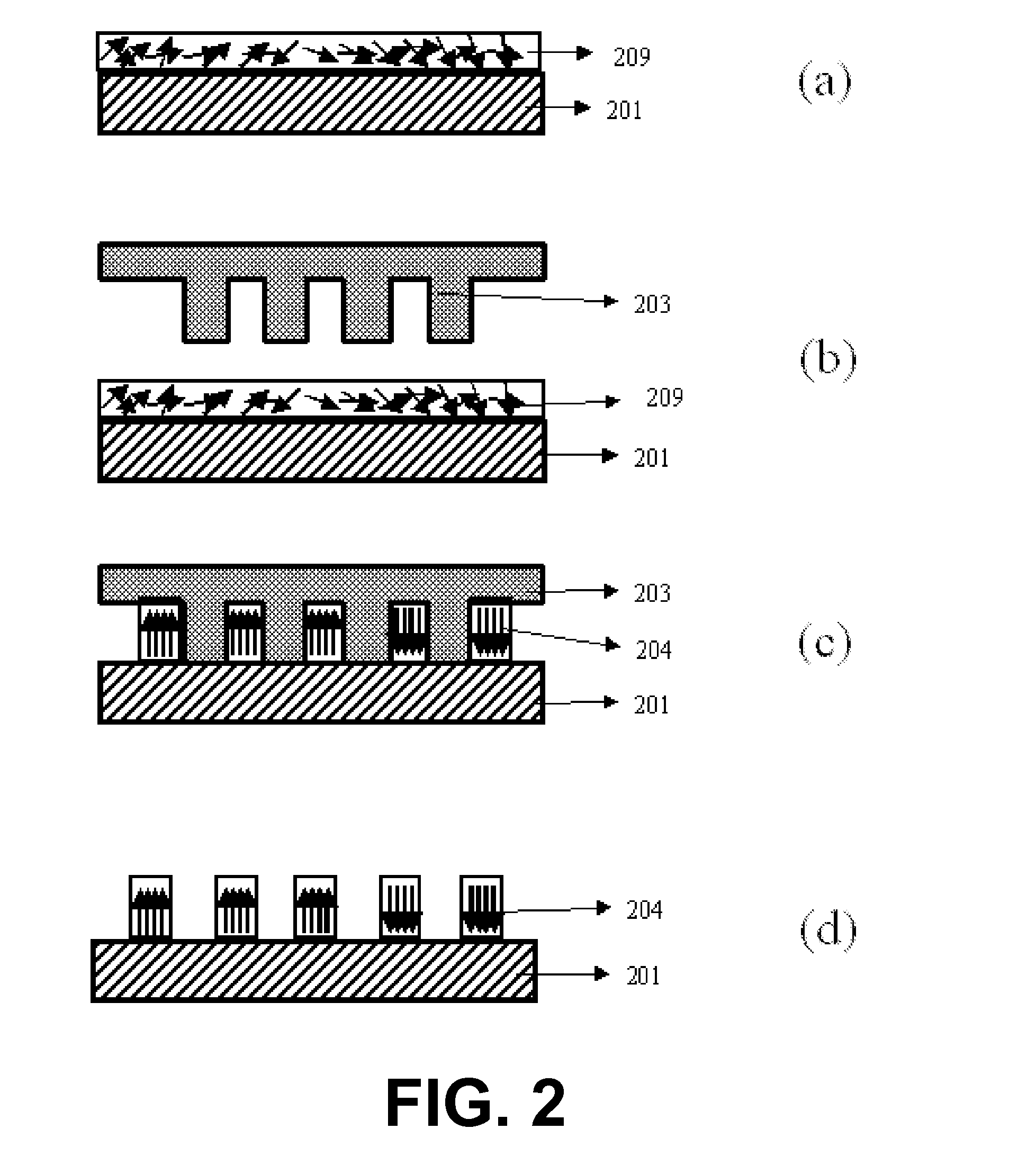
[0012]It is an advantage of embodiments of the present invention that a ferroelectric polymer material can be oriented in such a way as to align in the plane of the substrate the axis about which the dipolar moment rotates (i.e. the axis oriented in the same direction as the polymer chains also referred as the c-axis), without needing to apply an external electric field to obtain said orientation and therefore without degrading the interface between the electrode and the ferroelectric polymer material. This orientation results in optimal coupling between dipole moment and a vertical electric field (i.e. a field perpendicular to the substrate), and allows for easier rotation of the dipole moment.

Problems solved by technology

This process results in an elongated switching time under a given voltage due to the pinning of domain walls by structural defects.
However, the process typically results in the degradation of the interface between the electrode and polymer thin film, and thus to the deterioration of the ferroelectric properties.
However, investigations of the thickness dependence of the polarization behavior show a decline in the ferroelectric switching performance (for example, an increase of coercive field, a lower remnant polarization, and / or a longer switching time), when the film thickness is reduced to below 100 nm.
Such a high voltage is usually not available in microelectronic devices.
Unfortunately, none of the previously published methods or procedures is able to obtain this control over the orientation of polymer crystals and thus the c-axis.
Furthermore, the methods at present used for improving the ferroelectric properties of polymer memory devices are very tedious and labour-intensive.

Method used


Image

  • Ferroelectric organic memories with ultra-low voltage operation
  • Ferroelectric organic memories with ultra-low voltage operation
  • Ferroelectric organic memories with ultra-low voltage operation

Examples


Embodiment Construction

[0168]The present invention will be described with respect to particular embodiments and with reference to certain drawings but the invention is not limited thereto but only by the claims. The drawings described are only schematic and are non-limiting. In the drawings, the size of some of the elements may be exaggerated and not drawn on scale for illustrative purposes. The dimensions and the relative dimensions do not correspond to actual reductions to practice of the invention.

[0169]Furthermore, the terms first, second, third and the like in the description and in the claims, are used for distinguishing between similar elements and not necessarily for describing a sequence, either temporally, spatially, in ranking or in any other manner. It is to be understood that the terms so used are interchangeable under appropriate circumstances and that the embodiments of the invention described herein are capable of operation in other sequences than described or illustrated herein.

[0170]More...


PUM


Abstract

A method of manufacturing a patterned ferroelectric polymer memory medium is disclosed, which includes forming an electrode on a substrate; forming a ferroelectric polymer thin film on the electrode; and patterning and orienting the polymer thin film into a plurality of nanostructures by embossing techniques. Also disclosed are two methods which include forming nanofeatures in an interlayer dielectric (ILD) layer deposited on a substrate; forming a ferroelectric polymer thin film on the ILD layer in the nanofeatures; and patterning and orienting the polymer thin film into a plurality of nanostructures by pressing. The patterning process followed by an annealing process promotes specific crystal orientation, which significantly reduces the operation voltage, and increases the signal-to-noise ratio. The invention also covers devices made of a ferroelectric polymer layer oriented by such an embossing method and the use of such devices at a coercive field of 10 MV / m or less.

Description

FIELD OF THE INVENTION[0001]The present invention relates to the field of memory device and recording medium wfor use in microelectronics. In particular, the present invention relates to polymer material based, non-volatile ferroelectric memory devices, their manufacturing and their use.BACKGROUND ART[0002]It is known that ferroelectric thin films can be used as memory media for memory or data storage applications. Ferroelectric memory devices notably provide non-volatile capability, relatively low voltage operation, and fast switching speed, compared to other currently used memory or data storage media. One way to construct an electrically addressable ferroelectric memory device consists of combining a ferroelectric capacitor and a transistor (1C1T, a device known as FeRAM (ferroelectric random access memory)). Another way consists in integrating arrays of ferroelectric capacitors. FeRAMs exhibit the endurance of dynamic random access memories (DRAM), the fast write and read speed ...

Claims


Application Information

Patent Timeline
IPC IPC(8): H01L29/68H01L21/04
CPCH01L27/11502G11C11/22H10B53/00
Inventor JONAS, ALAINHU, ZHIJUN
Owner UNIVERSITE CATHOLIQUE DE LOUVAIN
Learn More