Method for manufacturing free-standing substrate and free-standing light-emitting device

a technology of free-standing substrates and light-emitting devices, which is applied in the direction of chemically reactive gases, crystal growth processes, chemistry apparatuses and processes, etc., can solve the problems of gan film defects, yield down or fragmentation, and increase the power consumption of a single led from several microwatts to 1 watt, 3 watts or even more than 5 watts, etc., to achieve uniform etching, poor repeatability, and not conductive to mass production

Inactive Publication Date: 2011-05-26
CHANG CHUNYEN
View PDF25 Cites 62 Cited by
  • Summary
  • Abstract
  • Description
  • Claims
  • Application Information

AI Technical Summary

Benefits of technology

[0062]As compared to the laser lift-off that uses laser to generate a high temperature (>600° C.) so as to decompose the interface between a growth substrate and a light-emitting layer, the present invention uses a chemical etching process with an operating temperature below 80° C. for separation, thereby avoiding that the high-temperature separation process causes damages to the resulting light-emitting device.
[0063]Also, as compared to the lift-off method disclosed in documents 5, 10, and 11, which grows GaN into a nanorod structure directly, the present invention does not have the following disadvantages: the nano-rods tend to have the lattice orientations in different phases due to being grown independently, the directly grown nano-rods have poor repeatability, and it is not conductive to mass production.
[0064]Furthermore, as compared to the method disclosed in document 6, which initiates etching from outside of the CrN buffer layer, the present invention forms the sacrificial layer into rod shape, so it is advantageous to allow the etchant flowing throughout the opened internal part of the sacrificial layer so as to have uniform etching.
[0065]Moreover, as compared to the void-assisted separation method disclosed in document 9, which uses

Problems solved by technology

However, since the sapphire is non-conductive and electrodes cannot be formed thereon, in the case of the formation of a vertical LED, a sapphire substrate is mostly and finally removed.
Moreover, with the brightness of LED die enhanced, the power consumption of a single LED is increased from several microwatts to 1 watt, 3 watts or even more than 5 watts.
Furthermore, an inappropriate coating or material selection will affect the adhesive effect of the bonding layer 108, and even cause defects generated in the GaN film.
When the laser focuses on the plane of layer and scans, the overlap or gap problem easily arises to cause an energy input on the scan interface overlapped or insufficient, resulting yield down or fragmentation.
Also, since the transient temperature on the separation interface reaches over 600° C., it is easy to cause damages to the device.
Moreover, due to the laser being expensive and having limited life time, it is difficult to reduce unit production cost.
However, in this method, the formed structure is attached to a fixture when cutting the epitaxial layers, so

Method used


Image

  • Method for manufacturing free-standing substrate and free-standing light-emitting device
  • Method for manufacturing free-standing substrate and free-standing light-emitting device
  • Method for manufacturing free-standing substrate and free-standing light-emitting device

Examples


embodiment 1

[0077]FIG. 4 is a flow chart explaining an embodiment of manufacturing a free-standing substrate of the present invention.

[0078]Referring to FIG. 5, a nitride film 204, an AlN film 206 (functioning as a sacrificial layer), and a nitride film 208 are sequentially grown on a sapphire substrate 202, and these three layers of films are defined as a first layer 210 having a sacrificial layer. A mask layer 212 is formed on the first layer.

[0079]Referring to FIG. 6, the mask layer 212 is patterned into a patterned mask layer 212a by photolithography.

[0080]Referring to FIG. 7, the first layer 210 is etched into a protrusion-like first layer 210a having a structure of a plurality of columns by using the patterned mask layer 212a as an etching mask, wherein the protrusion-like first layer 210a comprises a protrusion-like nitride layer 204a, a protrusion-like AlN film 206a, and a protrusion-like nitride layer 208a. Next, as shown in FIG. 8, the patterned mask layer 212a is removed.

[0081]Referr...

embodiment 2

[0083]Referring to FIG. 12, an InxAlyGa1-x-yN film (0≦x≦1, 0≦y≦1, x+y≦1) functioning as a sacrificial layer 306 is grown on a sapphire substrate 302. A mask layer 312 is formed on the sacrificial layer 306.

[0084]Referring to FIG. 13, the mask layer 312 is patterned into a patterned mask layer 312a by photolithography.

[0085]Referring to FIG. 14, the sacrificial layer 306 is etched into a protrusion-like sacrificial layer 306a having a structure of a plurality of protrusions by using the patterned mask layer 312a as an etching mask. Then, as shown in FIG. 15, the patterned mask layer 312a is removed.

[0086]Referring to FIG. 16, a nitride layer 320 is grown on the protrusion-like sacrificial layer 306a by epitaxial lateral overgrown.

[0087]Referring to FIG. 17, AZ400K (a mixture solution of KOH and H3BO3 as main components, manufactured by Clariant Company) is used as an etchant to etch away the protrusion-like sacrificial layer 306a, in order to separate the nitride layer 320 from the s...

embodiment 3

[0088]FIG. 19 is a flow chart explaining an embodiment of manufacturing a free-standing light-emitting device of the present invention.

[0089]Referring to FIG. 20, a nitride film 404, an AlN film 406 (functioning as a sacrificial layer), and a nitride film 408 are sequentially grown on a sapphire substrate 402, and these three layers of films are defined as a first layer 410 having a sacrificial layer. A mask layer 412 is formed on the first layer.

[0090]Referring to FIG. 21, the mask layer 412 is patterned into a patterned mask layer 412a by photolithography.

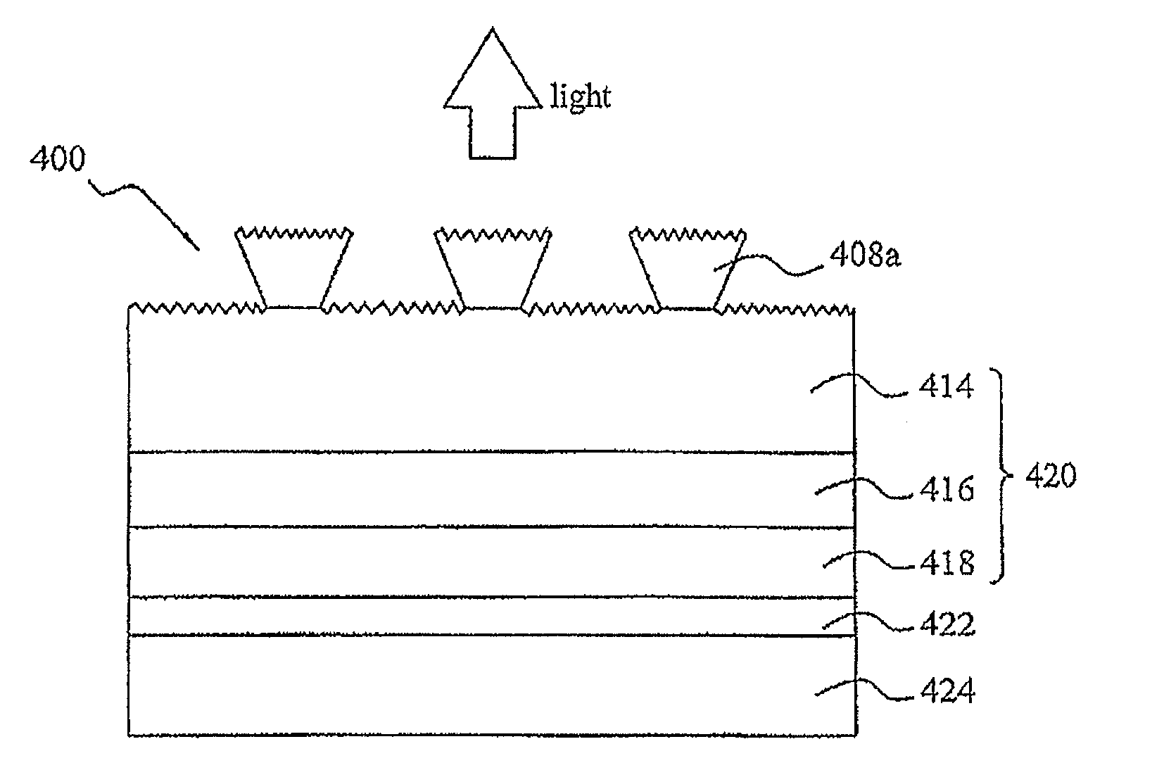
[0091]Referring to FIG. 22, the first layer 410 is etched into a protrusion-like first layer 410a having a structure of a plurality of protrusions by using the patterned mask layer 412a as an etching mask, wherein the protrusion-like first layer 410a comprises a protrusion-like nitride layer 404a, a protrusion-like AlN film 406a, and a protrusion-like nitride layer 408a. Next, as shown in FIG. 23, the patterned mask layer 412a is...


PUM


Abstract

The present invention provides a method for manufacturing a free-standing substrate, comprising: growing a first layer having a sacrificial layer on a growth substrate; patterning the first layer into a patterned first layer having a structure of a plurality of protrusions; growing a second layer on the patterned first layer having a structure of a plurality of protrusions by epitaxial lateral overgrowth; and separating the second layer from the growth substrate by etching away the sacrificial layer, wherein the separated second layer functions as a free-standing substrate for epitaxy. Also, the present invention provides a method for manufacturing a free-standing light-emitting device, comprising: growing a first layer having a sacrificial layer on a growth substrate; patterning the first layer into a patterned first layer having a structure of a plurality of protrusions; growing a second layer on the patterned first layer having a structure of a plurality of protrusions by epitaxy growth; forming a reflecting layer on the second layer; forming a conductive substrate on the reflecting layer; and separating the second layer, the reflecting layer, and the conductive substrate from the growth substrate by etching away the sacrificial layer, so as to form a free-standing light-emitting device.

Description

BACKGROUND OF THE INVENITON[0001]1. Field of the Invention[0002]The present invention relates to a method for manufacturing a free-standing substrate and a free-standing light-emitting device. In particular, the present invention relates to a method for manufacturing a free-standing substrate for use of subsequent epitaxy or a free-standing vertical light-emitting device by etching a sacrificial layer patterned into a plurality of protrusions to separate a growth substrate.[0003]2. Description of the Related Art[0004]A light-emitting diode (LED) is a semiconductor material, in which a p-type semiconductor, an n-type semiconductor, and a light-emitting layer are epitaxially grown on a substrate. For group III-V compound semiconductors, sapphire is mainly used as a growth substrate. However, since the sapphire is non-conductive and electrodes cannot be formed thereon, in the case of the formation of a vertical LED, a sapphire substrate is mostly and finally removed. Moreover, with the...

Claims


Application Information

Patent Timeline
IPC IPC(8): H01L33/02H01L21/02
CPCC30B25/18H01L21/02422H01L21/02439H01L21/02458H01L21/02505H01L21/02521H01L33/22H01L21/02639H01L21/0265H01L21/02664H01L33/007H01L33/0079H01L33/20H01L21/0254H01L33/0093
Inventor CHANG, CHUN-YEN
Owner CHANG CHUNYEN
Why Eureka
Try Eureka