Epitaxial Structures, Methods of Forming the Same, and Devices Including the Same

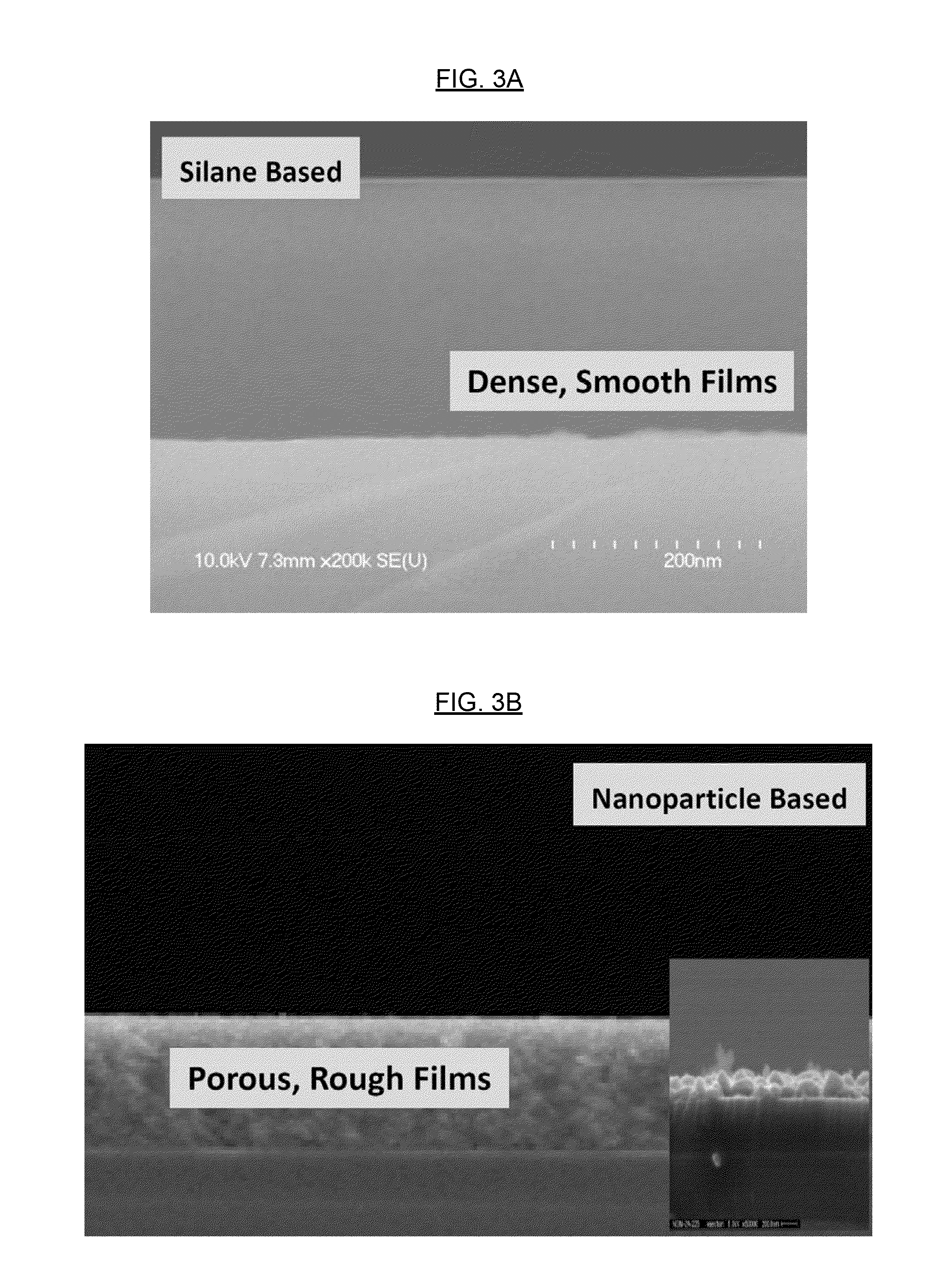
a technology of epitaxial structure and epitaxial structure, which is applied in the field of epitaxial structure, can solve the problems of limiting the extent of densification upon curing, affecting the electrical performance of such films, and producing relatively rough and porous films of silicon nanoparticles, etc., and achieves good film texture, density, conformality, and good film sintering properties. , good film in terms of texture and smoothness

Active Publication Date: 2011-10-06
ENSURGE MICROPOWER ASA
View PDF2 Cites 80 Cited by
  • Summary
  • Abstract
  • Description
  • Claims
  • Application Information

AI Technical Summary

Benefits of technology

[0006]Aspects of the present invention relate to epitaxial structures, methods of making epitaxial structures, and devices that utilize such epitaxial structures. The present epitaxial structures (which may be formed from a liquid-phase Group IVA semiconductor element ink comprising a (poly)silane, a (poly)germane, and / or a (poly)germasilane) may be advantageous because such inks form a relatively good film in terms of texture (smoothness), density, conformality, adhesion, electrical conductivity and purity when compared to similar films formed from a Group IVA semiconductor element nanoparticle-based ink. FIGS. 3A and 3B show cross-sectional electron microscope scans comparing cured silicon thin films made from (poly)silane-based ink and silicon nanoparticle-based ink, respectively. Specifically, as shown in FIG. 3A, the film formed from a (poly)silane-based ink is dense and smooth relative to the film(s) formed from silicon nanoparticle-based ink(s) (see, e.g., the film[s] shown in FIG. 3B). It is believed that the silicon nanoparticle-based ink produces a relatively rough and porous film because nanoparticles may have broad particle size distributions and do not always densify perfectly during sintering. Furthermore, silicon nanoparticles may carry a surface oxide and exhibit poor sintering properties, either one may lead to porous and / or rough films. In addition, nanoparticle ink formulations may require surface modification of silicon nanoparticles, may comprise dispersing agents to formulate a silicon nanoparticle ink, either one of which can introduce impurities into subsequently formed films which may further limit the extent of densification upon curing and affect the electrical performance of such films.

Problems solved by technology

It is believed that the silicon nanoparticle-based ink produces a relatively rough and porous film because nanoparticles may have broad particle size distributions and do not always densify perfectly during sintering.
Furthermore, silicon nanoparticles may carry a surface oxide and exhibit poor sintering properties, either one may lead to porous and / or rough films.
In addition, nanoparticle ink formulations may require surface modification of silicon nanoparticles, may comprise dispersing agents to formulate a silicon nanoparticle ink, either one of which can introduce impurities into subsequently formed films which may further limit the extent of densification upon curing and affect the electrical performance of such films.
A layer or feature to be grown epitaxially on a substrate cannot be formed from a Group IVA semiconductor element nanoparticle-based ink because of the nanocrystalline nature of such particles, leading to a multitude of surface defects and varying crystallographic phases and / or orientations, their largely random orientation relative to each other in a deposited film, and their typical poor sintering behavior, as outlined above.
Consequently, films formed from a Group IVA nanoparticle-based ink appear to be limited with regard to the formation of good quality epitaxial films, layers, and / or features, which may lead to the enhancement of properties such as power conversion efficiency and contact resistance that depend on the quality of the interface between the film and the material or substrate to which the film makes contact.

Method used


Image

  • Epitaxial Structures, Methods of Forming the Same, and Devices Including the Same
  • Epitaxial Structures, Methods of Forming the Same, and Devices Including the Same
  • Epitaxial Structures, Methods of Forming the Same, and Devices Including the Same

Examples


Embodiment Construction

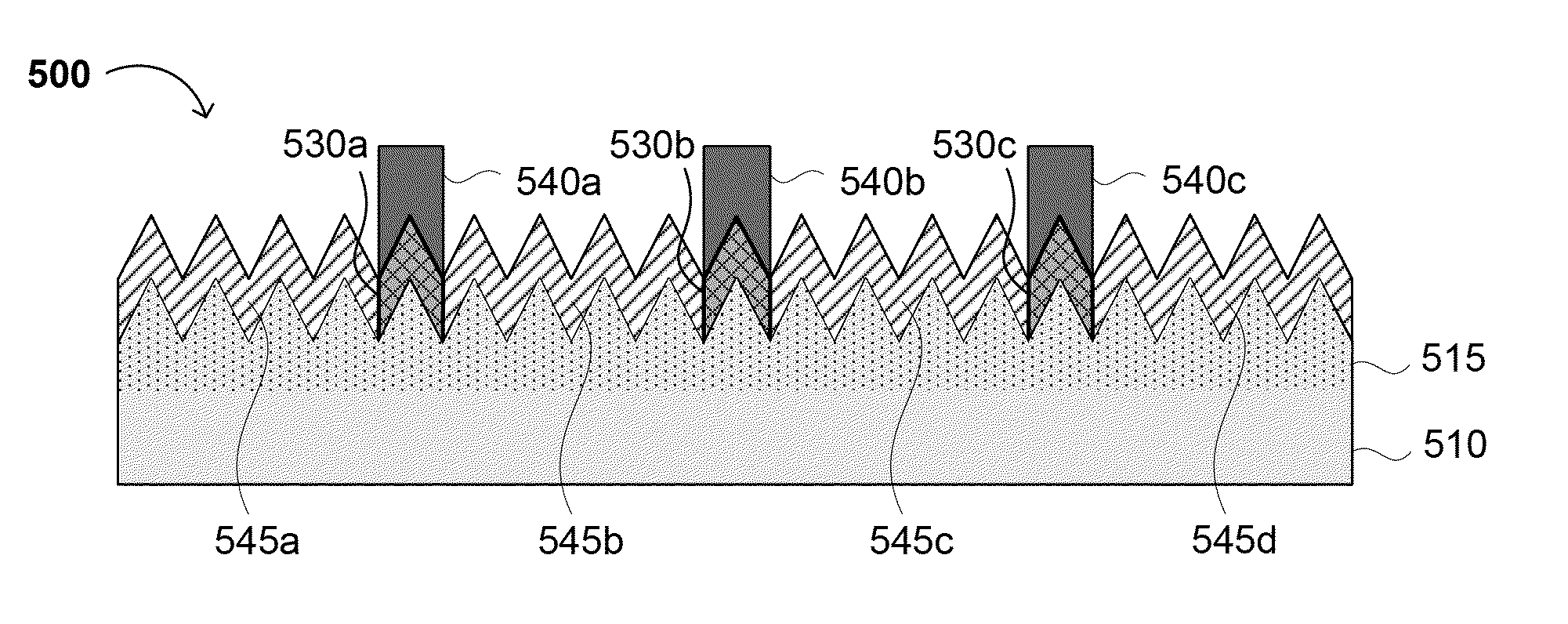
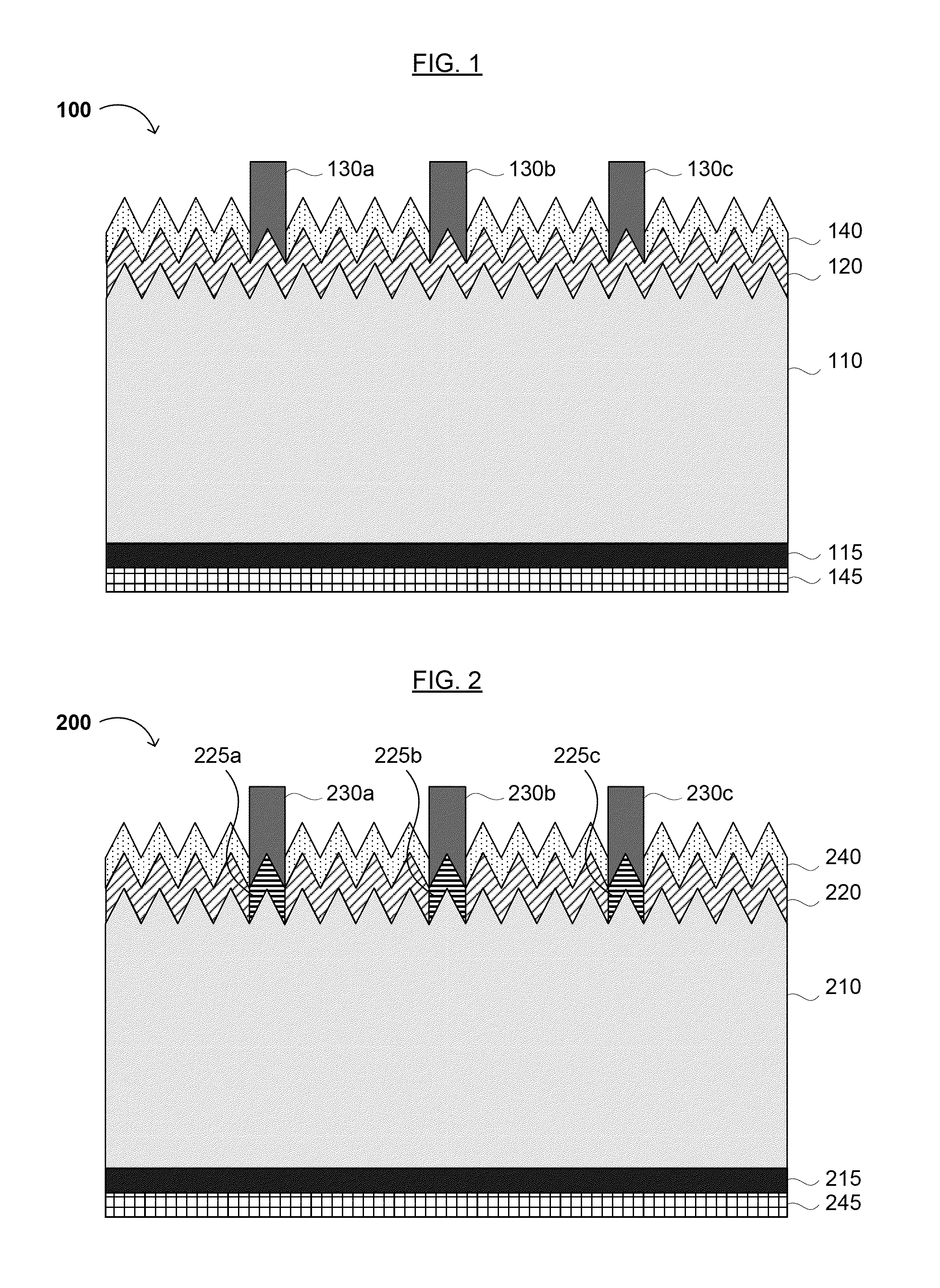
[0025]Reference will now be made in detail to various embodiments of the invention. While the invention will be described in conjunction with the following preferred embodiments, it will be understood that the description is not intended to limit the invention to these embodiments. On the contrary, the invention is intended to cover alternatives, modifications and equivalents that may be included within the spirit and scope of the invention as defined by the appended claims. Furthermore, in the following detailed description, numerous specific details are set forth in order to provide a thorough understanding of the present invention. However, it will be readily apparent to one skilled in the art that the present invention may be practiced without these specific details. In other instances, well-known methods, procedures, components, and circuits have not been described in detail so as not to unnecessarily obscure aspects of the present invention.

[0026]In the present disclosure, the...


PUM

PropertyMeasurementUnit
temperatureaaaaaaaaaa

Abstract

Epitaxial structures, methods of making epitaxial structures, and devices incorporating such epitaxial structures are disclosed. The methods and the structures employ a liquid-phase Group IVA semiconductor element precursor ink (e.g., including a cyclo- and/or polysilane) and have a relatively good film quality (e.g., texture, density and/or purity). The Group IVA semiconductor element precursor ink forms an epitaxial film or feature when deposited on a (poly)crystalline substrate surface and heated sufficiently for the Group IVA semiconductor precursor film or feature to adopt the (poly)crystalline structure of the substrate surface. Devices incorporating a selective emitter that includes the present epitaxial structure may exhibit improved power conversion efficiency relative to a device having a selective emitter made without such a structure due to the improved film quality and/or the perfect interface formed in regions between the epitaxial film and contacts formed on the film.

Description

RELATED APPLICATIONS[0001]This application claims the benefit of U.S. Provisional Application No. 61 / 321,458, filed on Apr. 6, 2010 (Attorney Docket No. IDR3701), which is incorporated herein by reference in its entirety.FIELD OF THE INVENTION[0002]The present invention generally relates to the field of materials and films for electronic applications. More specifically, embodiments of the present invention pertain to epitaxial structures, methods of forming epitaxial structures, and devices comprising epitaxial structures.BACKGROUND[0003]Selective emitters in solar cells (e.g., an emitter having very highly doped regions under metal contacts and having moderate to highly doped regions in other areas of the cell) are desirable because they allow for improved electrical conductivity between the metal contact and a P- or N-type doped region of the solar cell without negatively impacting light absorption of the cell in other areas when compared to a conventional solar cell without a sel...

Claims


Application Information

Patent Timeline
Patent Type & Authority Applications(United States)
IPC IPC(8): H01L29/04H01L21/20
CPCH01L21/0237H01L21/02428H01L21/0243H01L21/02494H01L21/02532Y02E10/547H01L21/02628H01L21/02661H01L31/068H01L31/1804H01L21/02587H01L21/228Y02P70/50H01L31/02161H01L31/02167
Inventor ROCKENBERGER, JOERGZURCHER, FABIOTAKASHIMA, MAO
Owner ENSURGE MICROPOWER ASA
Why Eureka
Try Eureka