Indium oxide sintered compact and sputtering target
a technology of indium oxide and compact, which is applied in the direction of diaphragms, metallic material coating processes, inorganic chemistry, etc., can solve the problems of inability to suitably use above transparent semiconductor thin films, inability to display high-speed animations or the like, and large amount of energy and a large number of steps, etc., to achieve excellent film-forming stability and excellent semiconductor films
- Summary
- Abstract
- Description
- Claims
- Application Information
AI Technical Summary
Benefits of technology
Problems solved by technology
Method used
Image

Examples
example 1
[0060]The following oxide powders were used as raw material powders. The specific surface area of each powder was measured by the BET method.
(a) Indium oxide powder (specific surface area: 6 m2 / g)
(b) Scandium oxide powder (specific surface area: 3 m2 / g)
The powder mixture had a specific surface area of 6.0 m2 / g.
[0061]A powder mixture of 990 g of indium oxide and 10 g of scandium oxide was mixed and ground using an agitator bead mill with a wet medium. Zirconia beads having a diameter of 1 mm were used as the media. The specific surface area of the raw material powder mixture was increased by 2 m2 / g by grinding while checking the specific surface area of the raw material powder mixture.
[0062]The ground powder mixture was dried using a spray dryer, put in a die (diameter: 100 mm, thickness: 20 mm), and pressed using a cold press machine.
[0063]The shaped product was sintered at 1500° C. for 20 hours in an oxygen atmosphere (in which oxygen was circulated) to obtain a sintered body.
[0064...
examples 2 to 5
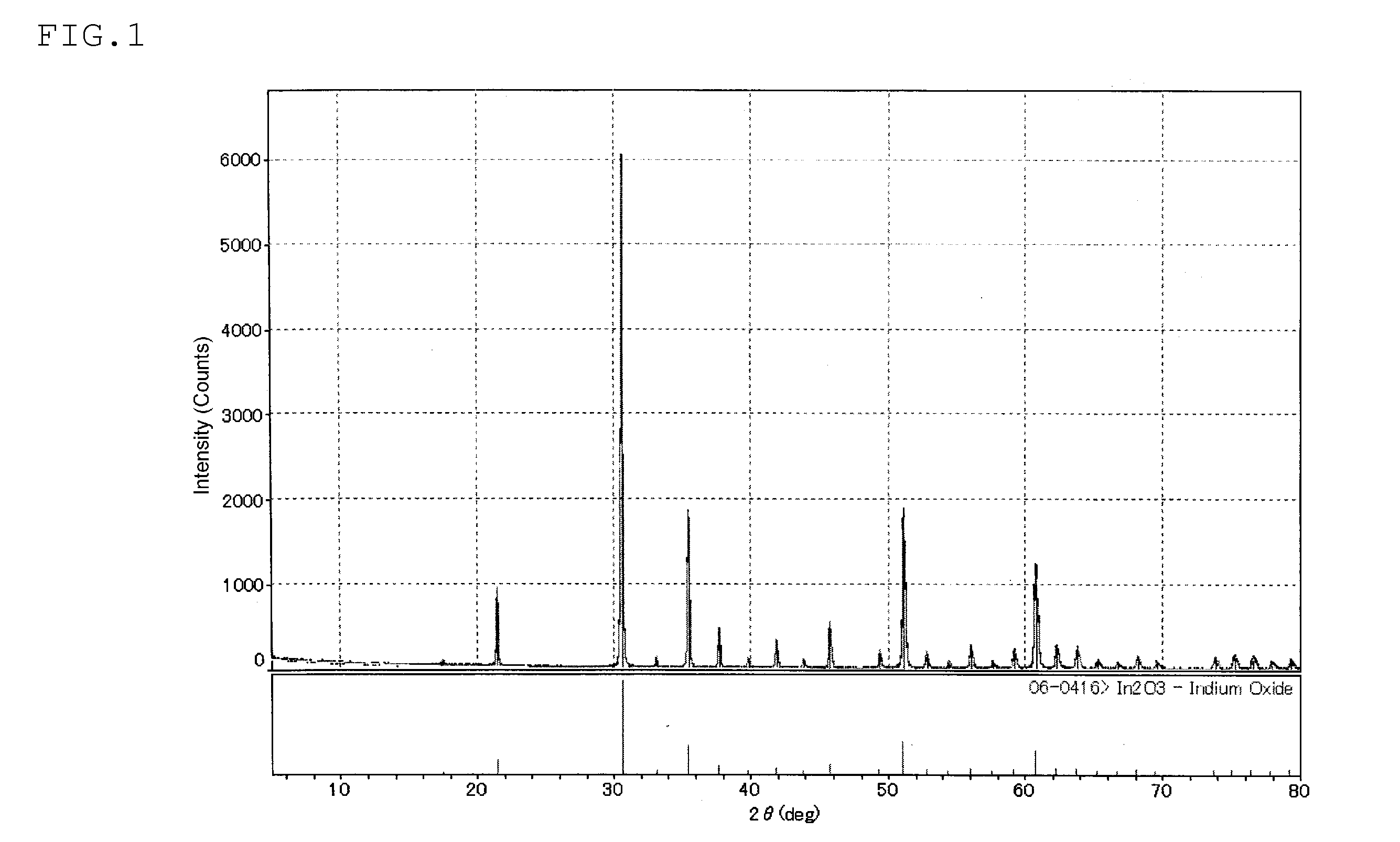
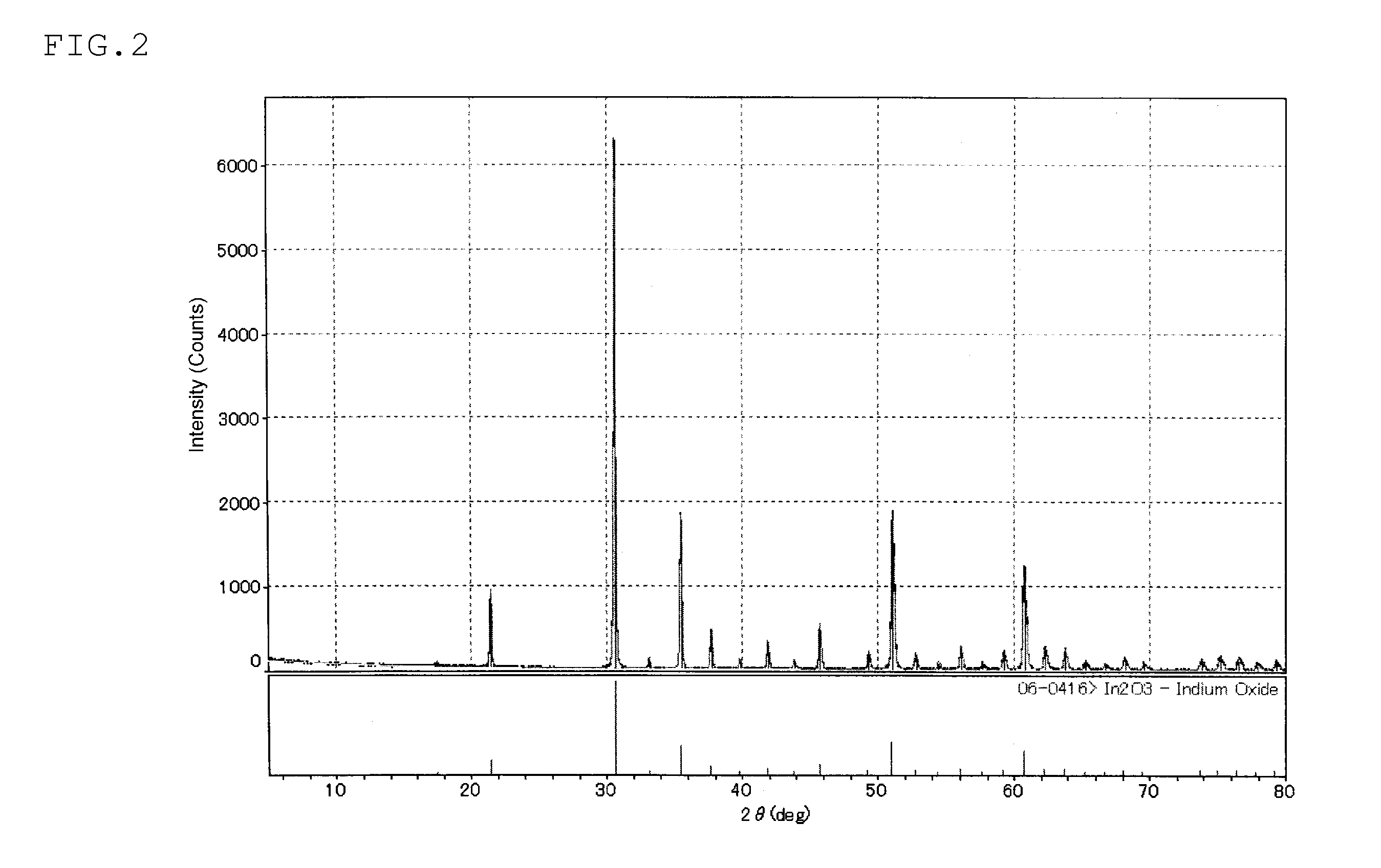
[0075]A sintered body was produced and evaluated in the same manner as in Example 1, except for changing the atomic ratio “Sc / (In +Sc)”, the sintering temperature, and the sintering time as shown in Table 1. The evaluation results are shown in Table 1. FIGS. 2 to 5 respectively show the X-ray diffraction charts of the sintered bodies produced in Examples 2 to 5.
[0076]Note that the measured lattice constant almost coincided with the theoretical lattice constant (see FIG. 9), and a peak attributed to Sc2O3 (raw material) was not observed even if the X-ray diffraction chart was magnified. It was thus confirmed that scandium oxide was solid-dissolved in the indium oxide crystal.
Example 6
[0077]A sintered body was produced in the same manner as in Example 2, except for using cerium oxide (CeO2) in addition to indium oxide and scandium oxide so that the Ce content was 800 atomic ppm or 1200 atomic ppm based on the total metal elements. The resulting sintered bodies had a density of 6.5 g / c...
example 6
[0097]The following oxide powders were weighed and used as raw material powders. The specific surface area of each powder was measured by the BET method.
(a) Indium oxide powder (specific surface area: 6 m2 / g)
(b) Aluminum oxide powder (specific surface area: 6 m2 / g)
A powder mixture of the powders (a) and (b) had a specific surface area of 6.0 m2 / g.
[0098]A powder mixture of 995 g of indium oxide and 5 g of aluminum oxide was mixed and ground using an agitator bead mill with a wet medium. Zirconia beads having a diameter of 1 mm were used as the media. The specific surface area of the raw material powder mixture was increased by 2 m2 / g by grinding while checking the specific surface area of the raw material powder mixture.
[0099]The ground raw material powder mixture was dried using a spray dryer, put in a die (diameter: 100 mm, thickness: 20 mm), and pressed using a cold press machine. The shaped product was sintered at 1550° C. for 20 hours in an oxygen atmosphere (in which oxygen was...
PUM
| Property | Measurement | Unit |
|---|---|---|
| grain size | aaaaa | aaaaa |
| temperature | aaaaa | aaaaa |
| grain size | aaaaa | aaaaa |
Abstract
Description
Claims
Application Information
 - R&D
- Intellectual Property
- Life Sciences
- Materials
- Tech Scout
- Unparalleled Data Quality
- Higher Quality Content
- 60% Fewer Hallucinations
Browse by: Latest US Patents, China's latest patents, Technical Efficacy Thesaurus, Application Domain, Technology Topic, Popular Technical Reports.
© 2025 PatSnap. All rights reserved.Legal|Privacy policy|Modern Slavery Act Transparency Statement|Sitemap|About US| Contact US: help@patsnap.com