

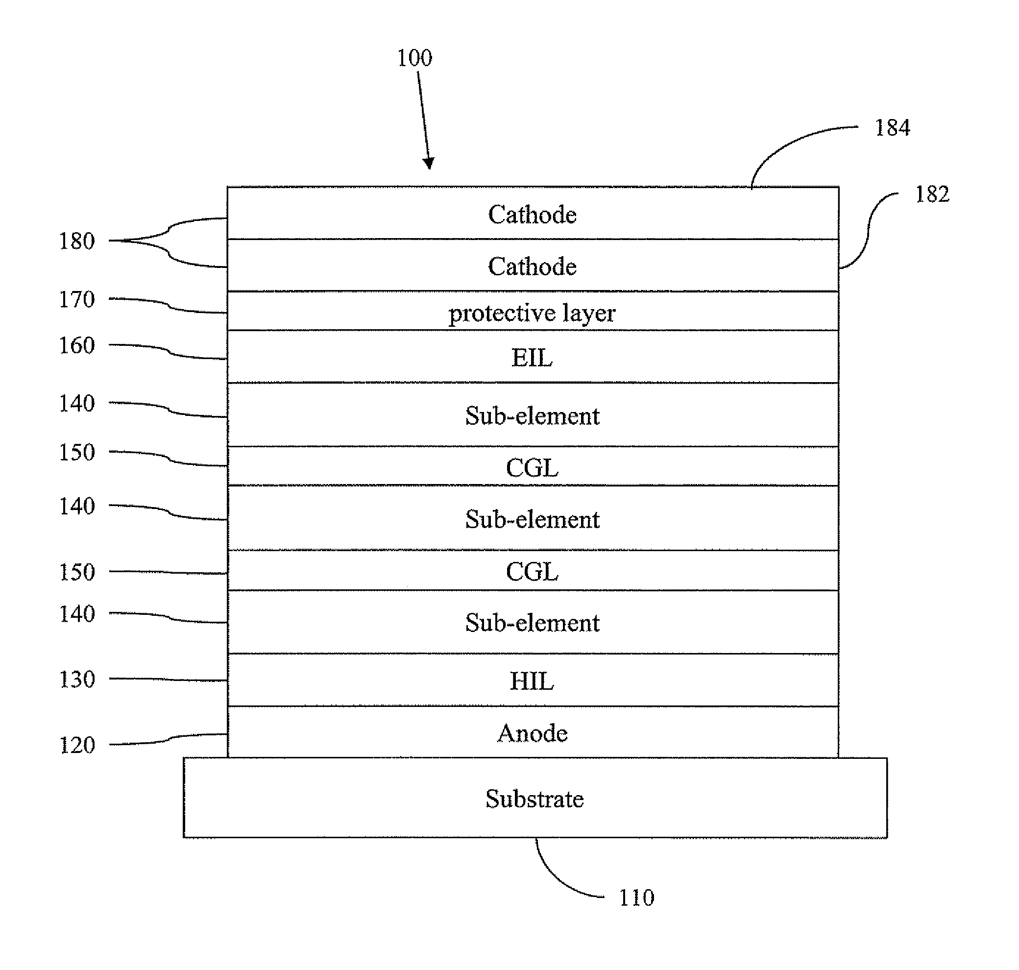
Stacked white OLED having separate red, green and blue sub-elements
a technology of white oled and sub-elements, which is applied in the field of white oleds or woleds, which can solve the problems of difficult combination of hosts and phosphorescent dopants
- Summary
- Abstract
- Description
- Claims
- Application Information
AI Technical Summary
Benefits of technology
Problems solved by technology
Method used
Image

Examples
example 1
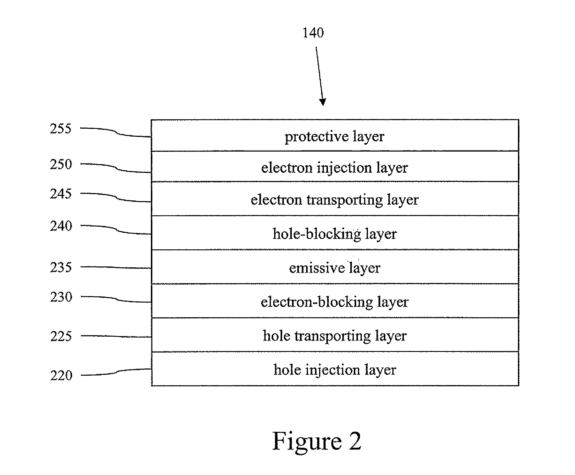
[0132]The 20 Ω / sq indium tin oxide precoated glass substrates were degreased in detergent solution and cleaned by solvents, followed by treatment for ten-minute with UV / ozone before being transferred to a high vacuum of 10-7 Torr. Then B, G, and R OLED sub-elements were sequentially deposited by thermal evaporation without breaking vacuum, with 10-nm BPhen layer doped with Li in a 1:1 molar ratio and a following 10-nm MoO3 spaced in between each sub-element. Lithium, an n-type dopant here, is to add impurities to transfer electrons to LUMO states. For each OLED sub-element, a 40-nm film of 4,4′- bis[N-(1-naphthyl)-N-phenyl-amino]-biphenyl (NPD) as the HTL was deposited, followed by 25-nm EML, and then an ETL of 50-nm-thick BPhen. Here, BPhen, instead of 2,9-dimethyl-4,7-diphenyl-1,10-phenanthroline (BCP), is used to reduce device drive voltage. Also note that in order to maintain good charge balance at high bias when charge leakage is not effectively prevented by energy barriers, th...
example 2
[0142]To further understand and optimize the CGL architecture, the charge generation in CGLs based on transparent metal oxides was systematically studied. The current density-voltage (J-V) and capacitance-voltage (C-V) characteristics was analyzed for electron- and hole-only devices consisting of MoO3 layers with varying thicknesses, and over a wide range of temperature. Optimized performance of a LiBCP / MoO3 CGL is demonstrated by varying both the thickness of MoO3, as well as the Li doping ratio in BCP. Thermally assisted tunneling from a trap level at (0.06±0.01)eV above the MoO3 valence band maximum into the adjacent organic layer is proposed to explain the temperature dependence of the J-V characteristics in both electron- and hole-only devices.
[0143]Both the electron- and hole-only devices were prepared on detergent and solvent cleaned glass substrates that were immediately transferred into a vacuum chamber with a base pressure of 10-7 Torr after a 10-minute exposure to a UV / oz...
example 3
[0155]To determine the effects of the charge generation efficiency on the performance of a green emitting SOLED with more than two sub-elements, OLEDs using the CGL as either a cathode (Cell-L), an anode (Cell-R), or both (Cell-M) were fabricated (see FIG. 20a), as well as the control device with an ITO anode / A1 cathode combination. Detailed structures are provided in Table III. Note that for Cell-R and Cell-M, 20 Å-thick Al was directly deposited onto ITO to ensure band alignment at the metal / organic interface, and thus to decrease the significant energy barrier that prevents electron transport from the CGL to ITO.
TABLE IIIStructure of the subcells in a 3 layer SOLED, and the control OLED.LayerDevicesFunctionsMaterialsThicknesses (Å)Cell-LanodeITO1500 HTLNPD400EMLIr(ppy)3:CBP250ETLBCP500CGLLi:BCP / MoO3100 / 100cathodeAl500Cell-ManodeITO / Al1500 / 20 CGLLi:BCP / MoO3100 / 100HTLNPD400EMLIr(ppy)3:CBP250ETLBCP500CGLLi:BCP / MoO3100 / 100cathodeAl500Cell-RanodeITO / Al1500 / 20 CGLLi:BCP / MoO3100 / 100HTLN...
PUM
 Abstract
Description
Claims
Application Information