Rolled Copper Foil or Electrolytic Copper Foil for Electronic Circuit, and Method of Forming Electronic Circuit Using Same

a technology of electrolytic copper foil and electronic circuit, which is applied in the direction of manufacturing tools, semiconductor/solid-state device details, transportation and packaging, etc., can solve the problems of copper circuit shortening, circuit not having the intended circuit width, and defective circuit, so as to shorten the time of forming circuit, prevent sagging, and inhibit oxidation

Inactive Publication Date: 2011-10-27
JX NIPPON MINING& METALS CORP
View PDF0 Cites 12 Cited by
  • Summary
  • Abstract
  • Description
  • Claims
  • Application Information

AI Technical Summary

Benefits of technology

[0037]The present invention yields the effect of being able to form a more uniform circuit having an intended circuit width upon forming a circuit by etching a copper foil of a copper-clad laminate. The present invention yields the additional effects of being able to prevent sagging caused by the etching, shorten the time of forming a circuit by etching, make the thickness of the nickel or nickel alloy layer as thin as possible, inhibit oxidation when exposed to heat, and prevent tarnish known as “YAKE”.
[0038]It is thereby possible to provide a rolled copper foil or electrolytic copper foil for an electronic circuit capable of improving the etching properties in pattern etching and preventing the occurrence of short circuits and defects in the circuit width, and further provide a method of forming a superior electronic circuit.

Problems solved by technology

However, when forming a circuit by etching, there is a problem in that the circuit does not have the intended circuit width.
This is because the copper portion of the copper foil circuit after etching is etched downward from the surface of the copper foil; that is, etched broader toward the resin layer (cause sagging).
If large “sagging” occurs, the copper circuit will short in the vicinity of the resin substrate, and may become defective.
Nevertheless, in the foregoing case, if there is a portion that has already reached a predetermined width dimension, such portion will be additionally etched, and the circuit width of that copper foil portion will correspondingly become narrower, and the uniform line width (circuit width) that is intended in the circuit design cannot be obtained.
In particular, there is a problem in that such portion (thinned portion) will generate heat and, in certain cases, become disconnected.
Under circumstances where the patterns of electronic circuits are becoming finer, problems caused by this kind of defective etching are still often encountered today, and are becoming major issues in forming circuits.
Here, some problems arose at the stage of making further improvements.
With respect to the latter, since it is exposed to heat, the nickel or nickel alloy layer is oxidized (commonly called “YAKE (oxidation)” since tarnish occurs), and there are problems in that the etching properties may deteriorate in the pattern etching, and defects such as short circuits or deterioration in the controllability of the circuit width may occur due to the deterioration in the resist coating properties (uniformity, adhesion) or the excessive etching of the interfacial oxide during the etching process.
Nevertheless, since these technologies were not proposed to prevent or inhibit the etching portion of the copper foil from being etched broader from the surface of the copper foil downward (occurrence of sagging) upon designing a copper foil circuit through etching, they are unable to resolve the foregoing problems.Patent Document 1: Japanese Laid-Open Patent Publication No. 2002-176242Patent Document 2: Japanese Laid-Open Patent Publication No.

Method used


Image

  • Rolled Copper Foil or Electrolytic Copper Foil for Electronic Circuit, and Method of Forming Electronic Circuit Using Same
  • Rolled Copper Foil or Electrolytic Copper Foil for Electronic Circuit, and Method of Forming Electronic Circuit Using Same

Examples


example 1

[0164]An electrolytic copper foil of 5 μm was used. The surface roughness Rz of the electrolytic copper foil was 3 μm. Under the foregoing nickel-zinc alloy plating (part 1) conditions, a nickel-zinc alloy plated layer of 390 μg / dm2 was formed on the gloss (S) surface of the electrolytic copper foil.

[0165]As shown in Table 1, the nickel content was 350 μg / dm2 and the zinc content was 40 μg / dm2 in the nickel-zinc alloy plated layer. The nickel ratio was 90 wt %. The copper foil was bonded to a resin substrate with the adhesive surface opposite to the surface provided with the nickel-zinc alloy plated layer.

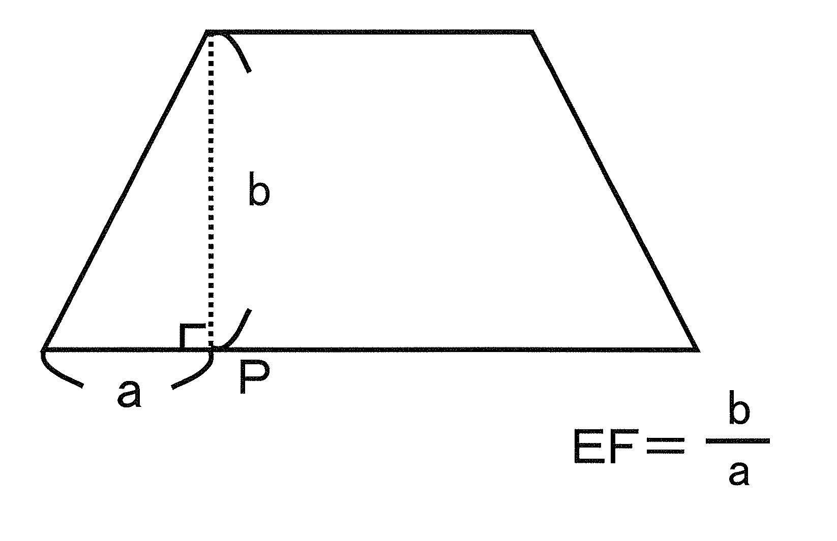
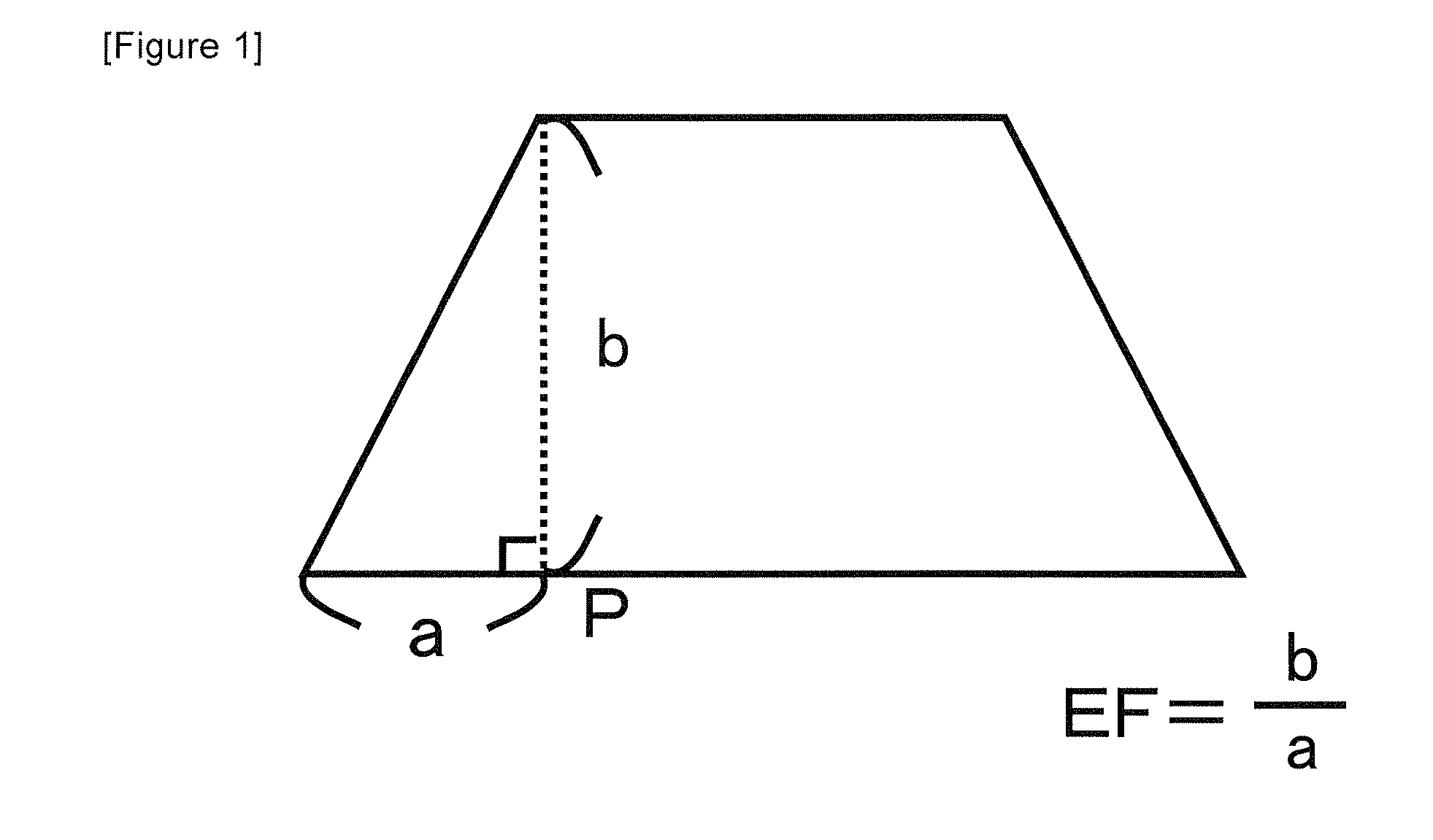
[0166]Subsequently, a circuit with 10 lines was printed with the process steps of resist coating and exposure, and etching treatment was further performed to remove any unwanted part of the copper foil. The etching conditions, circuit forming conditions, measurement conditions of the etching factor, and YAKE experiment were as follows.

(Etching Conditions)

[0167]Aqueous ferric chlori...

example 2

[0182]A rolled copper foil with a foil thickness of 18 μm was used. The surface roughness Rz of the rolled copper foil was 0.7 μm. Under the foregoing nickel-zinc alloy plating (part 2) conditions, a nickel-zinc alloy plated layer of 2150 μg / dm2 was formed on the rolled copper foil.

[0183]As shown in Table 1, the nickel content was 1500 μg / dm2 and the zinc content was 650 μg / dm2 in the nickel-zinc alloy plated layer. The nickel ratio was 70 wt %.

[0184]Moreover, the copper foil was bonded to a resin substrate with the adhesive surface opposite to the surface provided with the nickel-zinc alloy plated layer.

[0185]Subsequently, as with Example 1, a circuit with 10 lines was printed with the process steps of resist coating and exposure, and etching treatment was further performed to remove any unwanted part of the copper foil.

[0186]The etching conditions, measurement conditions of the etching factor, and YAKE experiment, but excluding the circuit forming conditions, were the same as Exam...

example 3

[0193]A rolled copper foil with a foil thickness of 18 μm was used. The surface roughness Rz of the rolled copper foil was 0.7 μm. Under the foregoing nickel-cobalt-zinc alloy plating conditions, a nickel-cobalt-zinc alloy plated layer was formed on the rolled copper foil. Here, the amount substituted with cobalt was 8% of the nickel amount based on nickel conversion.

[0194]As shown in Table 1, the nickel content was 2500 μg / dm2 and the zinc content was 300 μg / dm2 in the nickel-cobalt-zinc alloy layer. The nickel ratio was 89 wt %. This nickel ratio means a total amount of cobalt and nickel based on nickel conversion.

[0195]Moreover, the copper foil was bonded to a resin substrate with the adhesive surface opposite to the surface provided with the nickel-cobalt-zinc alloy plated layer.

[0196]Subsequently, as with Example 1, a circuit with 10 lines was printed with the process steps of resist coating and exposure, and etching treatment was further performed to remove any unwanted part o...


PUM

PropertyMeasurementUnit
inclination angleaaaaaaaaaa

Abstract

Provided is a rolled copper foil or electrolytic copper foil for an electronic circuit to be used for forming a circuit by etching, wherein the rolled copper foil or the electrolytic copper foil comprises a nickel alloy layer with lower etching rate than copper, which is formed on an etching side of the copper foil, and the nickel alloy layer contains zinc. This invention aims to prevent sagging caused by the etching, to form a uniform circuit having the intended circuit width, and to shorten the time of forming a circuit by etching as much as possible, when forming a circuit by etching a copper foil of the copper-clad laminate; and also aims to make the thickness of the nickel alloy layer as thin as possible, to inhibit oxidation when exposed to heat, to prevent tarnish (discoloration) known as “YAKE”, to improve the etching properties in pattern etching, and to prevent the occurrence of short circuits and defects in the circuit width.

Description

TECHNICAL FIELD[0001]The present invention relates to a rolled copper foil or electrolytic copper foil for an electronic circuit to be used for forming a circuit by etching, and to a method of forming an electronic circuit by using such rolled copper foil or electrolytic copper foil.BACKGROUND ART[0002]A copper foil for a printed circuit is being widely used in electronic devices and electrical equipment. This kind of copper foil for a printed circuit is generally bonded to a base material such as a synthetic resin board or a film with an adhesive or without using an adhesive under high temperature and pressure to produce a copper-clad laminate, a circuit is subsequently printed with the process steps of resist coating and exposure in order to form the intended circuit, etching treatment is further performed in order to remove any unwanted part of the copper foil, and various elements are soldered thereto in order to form a printed circuit for electronic devices.[0003]A copper foil ...

Claims


Application Information

Patent Timeline
Patent Type & Authority Applications(United States)
IPC IPC(8): H05K3/00B32B15/04B21C1/00
CPCB32B15/01Y10T428/12229C23F1/02C23F1/18C23F1/28C25D3/562C25D5/12C25D5/48C25D7/0614H05K3/06H05K3/067H05K3/384H05K2201/0338H05K2201/0355H05K2203/0723C23C22/24Y10T428/31678C25D7/06H05K1/09
Inventor YAMANISHI, KEISUKEKAMINAGA, KENGOFUKUCHI, RYO
Owner JX NIPPON MINING& METALS CORP
Why Eureka
Try Eureka