This helps you quickly interpret patents by identifying the three key elements:
Problems solved by technology
Method used
Benefits of technology
Benefits of technology
[0028]The effect of the invention disclosed in this specification can be easily understood in consideration of the following, but the following description is just one consideration.
[0029]When a positive voltage is applied to a gate electrode of a transistor, an electric field is generated from a gate electrode side of an oxide semiconductor layer to a back channel side (the side opposite to a gate insulating film). Therefore, hydrogen ions having positive charge which exist in the oxide semiconductor layer are transferred to the back channel side, and accumulated at the oxide semiconductor layer side of the interface between the oxide semiconductor layer and an insulating layer. The positive charge is transferred from the accumulated hydrogen ions to charge trapping centers (such as a hydrogen atom, water, or contamination) in the insulating layer, whereby negative charge is accumulated at the back channel side of the oxide semiconductor layer. In other words, a parasitic channel is generated at the back channel side of the transistor, and the threshold voltage is shifted to the negative side, so that the transistor tends to be normally-on.
[0030]In this manner, the charge trapping center such as hydrogen or water in the insulating layer traps the positive charge and the positive charge is transferred into the insulating layer, whereby the electrical characteristics of the transistor change. Accordingly, in order to suppress variation in the electrical characteristics of the transistor, it is important that there is no charge trapping centers or the number of the charge trapping centers is small in the insulating layer. Therefore, when the insulating layer is formed, a sputtering method which causes less hydrogen contained in the formed insulating layer is preferably used. In an insulating layer formed by a sputtering method, there is no charge trapping centers or a small number of charge trapping centers, and the transfer of positive charge does not easily occur as compared to the case of using a CVD method or the like. Therefore, the shift of the threshold voltage of the transistor can be suppressed, and the transistor can be normally-off.
[0031]Note that in a top-gate transistor, when an oxide semiconductor layer is formed over an insulating layer serving as a base and then heat treatment is performed thereon, not only water or hydrogen contained in the oxide semiconductor layer but also water or hydrogen contained in the insulating layer can be removed. Accordingly, in the insulating layer, there are a small number of charge trapping centers for trapping positive charge transferred through the oxide semiconductor layer. In this manner, since the heat treatment for dehydration or dehydrogenation is also performed on the insulating layer located below the oxide semiconductor layer in addition to the oxide semiconductor layer, in the top-gate transistor, the insulating layer serving as a base may be formed by a CVD method such as a plasma CVD method.
[0032]Note that in a bottom-gate transistor, when an oxide semiconductor layer is formed over a gate insulating layer and then heat treatment is performed thereon, not only water or hydrogen contained in the oxide semiconductor layer but also water or hydrogen contained in the gate insulating layer can be removed. Accordingly, in the gate insulating layer, there are a small number of charge trapping centers for trapping positive charge transferred through the oxide semiconductor layer. In this manner, since the heat treatment for dehydration or dehydrogenation is also performed on the gate insulating layer located below the oxide semiconductor layer in addition to the oxide semiconductor layer, in the bottom-gate transistor, the gate insulating layer may be formed by a CVD method such as a plasma CVD method.
[0033]In addition, when a negative voltage is applied to the gate electrode, an electric field is generated from the back channel side to the gate electrode side in the oxide semiconductor layer. Thus, hydrogen ions which exist in the oxide semiconductor layer are transferred to the gate insulating layer side and accumulated at the oxide semiconductor layer side of the interface between the oxide semiconductor layer and the gate insulating layer. As a result, the threshold voltage of the transistor is shifted to the negative side.
Problems solved by technology
However, the electric conductivity of an oxide semiconductor changes when deviation from the stoichiometric composition due to excess or deficiency of oxygen or the like occurs, or hydrogen or moisture forming an electron donor enters the oxide semiconductor, during a manufacturing process of a device.
In an insulating layer formed by a sputtering method, there is no charge trapping centers or a small number of charge trapping centers, and the transfer of positive charge does not easily occur as compared to the case of using a CVD method or the like.
Optical energy or BT stress detaches a hydrogen ion from an M-H bond, which causes deterioration; however, in the case where oxygen is implanted by the above-described doping, implanted oxygen is bonded to a hydrogen ion, so that an OH group is formed.
The OH group does not discharge a hydrogen ion even by light irradiation or application of BT stress on the transistor because of its high bond energy, and is not easily transferred in the oxide semiconductor layer because of its larger mass than the mass of a hydrogen ion.
It can be assumed that this is because an oxygen defect in the oxide semiconductor layer is one cause of the variation in the threshold voltage and the number of oxygen defects increases as the thickness of the oxide semiconductor layer is increased.
Method used
Image
Click on the blue label to locate the original text in one second.
Reading with bidirectional positioning of images and text.
Examples
embodiment 1
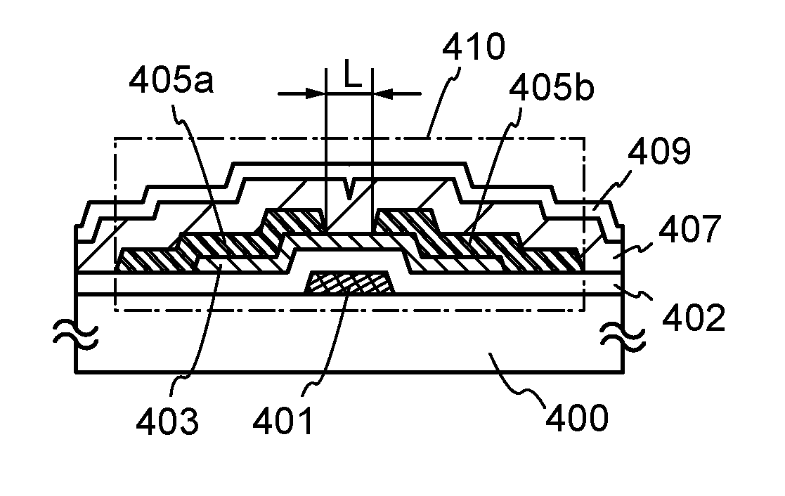
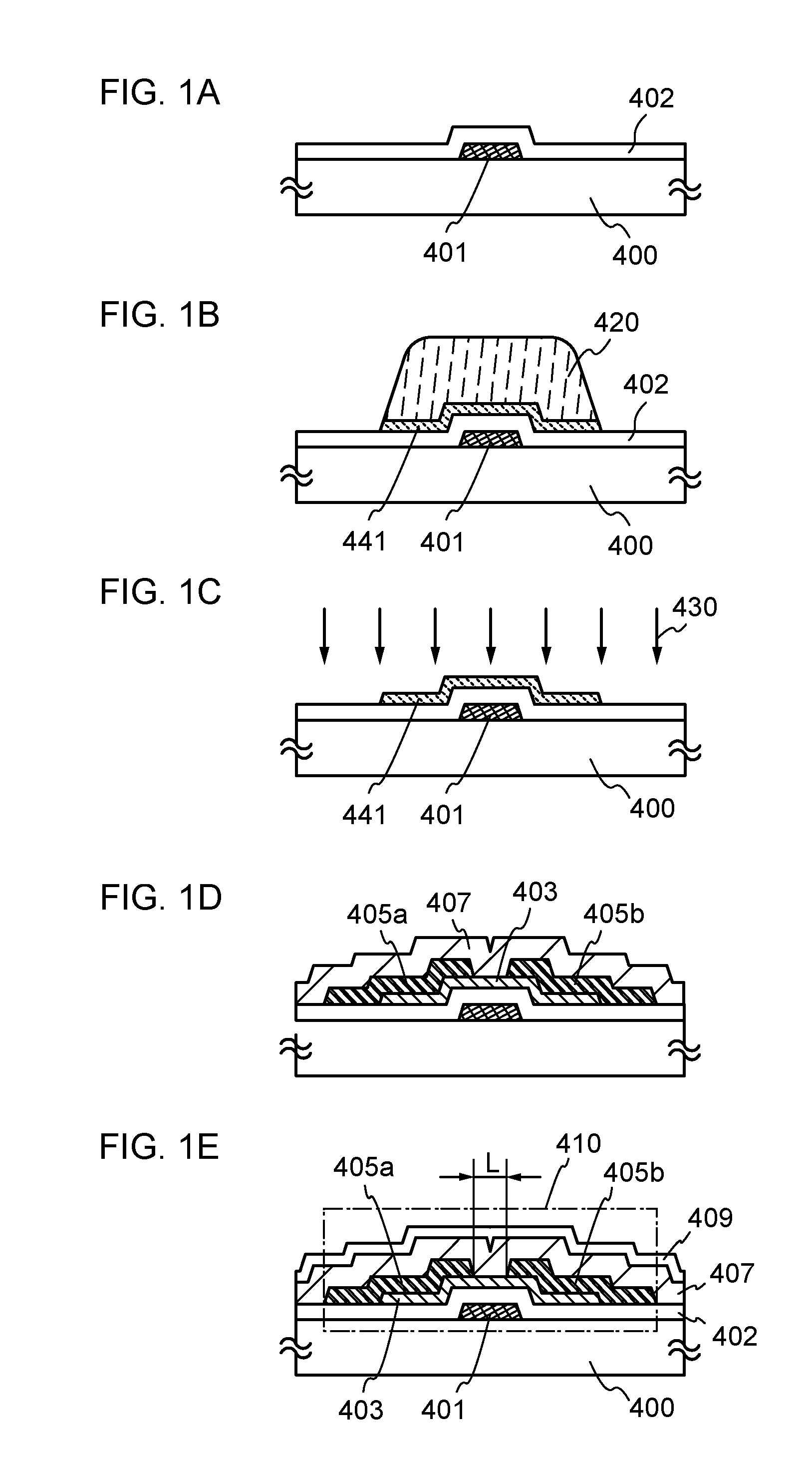
[0065]In this embodiment, an embodiment of a semiconductor device and a method for manufacturing the semiconductor device will be described with reference to FIGS. 1A to 1E and FIG. 5A. In this embodiment, as an example of the semiconductor device, a transistor including an oxide semiconductor for a semiconductor layer in which a channel is formed will be described in detail.
[0066]A transistor 410 illustrated in FIG. 1E includes, over a substrate 400, a gate electrode layer 401, a gate insulating layer 402, an oxide semiconductor layer 403, a source electrode layer 405a, and a drain electrode layer 405b. An insulating layer 407 (also referred to as a first insulating layer) and a protective insulating layer 409 (also referred to as a second insulating layer) are stacked over the transistor 410 in this order. The transistor 410 is one of bottom-gate transistors, and is also one of inverted staggered transistors.
[0067]FIGS. 1A to 1E illustrate an example of a method for manufacturing ...
embodiment 2
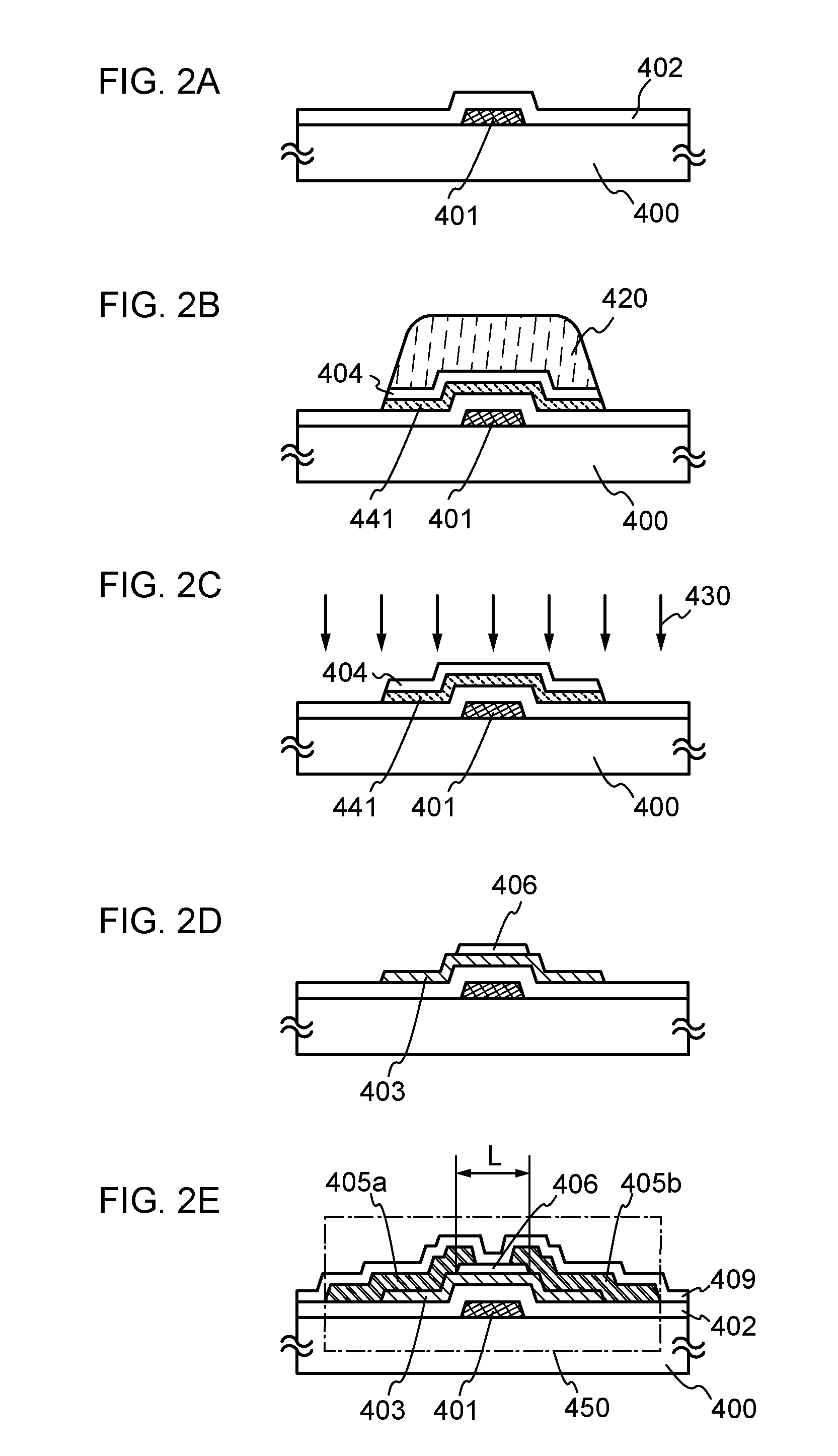
[0163]In this embodiment, another embodiment of a semiconductor device and a method for manufacturing the semiconductor device will be described with reference to FIGS. 2A to 2E and FIG. 5B. Note that the same portions or portions having similar functions as in Embodiment 1 can be formed as in Embodiment 1, and the same steps or similar steps as in Embodiment 1 can be performed as in Embodiment 1; therefore, the description is not repeated in this embodiment. In addition, detailed description of the same portions is not repeated, either.
[0164]A transistor 450 illustrated in FIG. 2E includes, over a substrate 400, a gate electrode layer 401, a gate insulating layer 402, an oxide semiconductor layer 403, a channel protective layer 406, a source electrode layer 405a, and a drain electrode layer 405b. A protective insulating layer 409 is formed over the transistor 450. In addition, an insulating layer 407 may be provided as in the transistor 410. The transistor 450 has a kind of bottom-...
embodiment 3
[0198]In this embodiment, another embodiment of a semiconductor device and a method for manufacturing the semiconductor device will be described with reference to FIGS. 3A to 3E and FIG. 5C. Note that the same portions or portions having similar functions as in the above embodiment can be formed as in the above embodiment, and the same steps or similar steps as in the above embodiment can be performed as in the above embodiment; therefore, the description is not repeated in this embodiment. In addition, detailed description of the same portions is not repeated, either.
[0199]A transistor 460 illustrated in FIG. 3E includes, over a substrate 400, a source electrode layer 405a, a drain electrode layer 405b, an oxide semiconductor layer 403, a gate insulating layer 402, and a gate electrode layer 401. A base layer 436 is formed between the substrate 400 and the oxide semiconductor layer 403. A protective insulating layer 409 is provided over the transistor 460. A cap layer 404 is formed...
PUM
Abstract
A semiconductor device including an oxidesemiconductor with stable electric characteristics and high reliability is provided. An island-shaped oxidesemiconductor layer is formed by using a resistmask, the resistmask is removed, oxygen is introduced (added) to the oxide semiconductor layer, and heat treatment is performed. The removal of the resistmask, introduction of the oxygen, and heat treatment are performed successively without exposure to the air. Through the oxygen introduction and heat treatment, impurities such as hydrogen, moisture, a hydroxyl group, or hydride are intentionally removed from the oxide semiconductor layer, whereby the oxide semiconductor layer is highly purified. Chlorine may be introduced to an insulating layer over which the oxide semiconductor layer is formed before formation of the oxide semiconductor layer. By introducing chlorine, hydrogen in the insulating layer can be fixed, thereby preventing diffusion of hydrogen from the insulating layer into the oxide semiconductor layer.
Description
TECHNICAL FIELD[0001]An embodiment of the present invention relates to a semiconductor device and a method for manufacturing the semiconductor device.[0002]Note that in this specification, a semiconductor device refers to any device that can function by utilizing semiconductor characteristics, and an image pick-up device, a display device, an electro-optical device, a power supply device, a semiconductor circuit, and an electronic device are all semiconductor devices.BACKGROUND ART[0003]Attention has been focused on a technique for forming a transistor (also referred to as a thin film transistor (TFT)) using a semiconductor thin film formed over a substrate having an insulating surface. The transistor is applied to a wide range of electronic devices such as an integrated circuit (IC) or an image display device (display device). A silicon-based semiconductor material is widely known as a material for a semiconductor thin film applicable to the transistor. As another material, an oxid...
Claims
Application Information
Patent Timeline
Application Date:The date an application was filed.
Publication Date:The date a patent or application was officially published.
First Publication Date:The earliest publication date of a patent with the same application number.
Issue Date:Publication date of the patent grant document.
PCT Entry Date:The Entry date of PCT National Phase.
Estimated Expiry Date:The statutory expiry date of a patent right according to the Patent Law, and it is the longest term of protection that the patent right can achieve without the termination of the patent right due to other reasons(Term extension factor has been taken into account ).
Invalid Date:Actual expiry date is based on effective date or publication date of legal transaction data of invalid patent.

