Semiconductor device and snubber device

a technology of snubber device and semiconductor, applied in the direction of snubber device details, emergency protective arrangement for limiting excess voltage/current, pulse technique, etc., can solve the problems of increasing cost and effort, increasing the size of applications, etc., and achieve the effect of reducing the cost of heat dissipation design and wiring design

Active Publication Date: 2011-12-22
MITSUBISHI ELECTRIC CORP
View PDF6 Cites 21 Cited by
  • Summary
  • Abstract
  • Description
  • Claims
  • Application Information

AI Technical Summary

Benefits of technology

[0007]An object of the present invention is to provide a semiconductor device including a snubber device which suppress costs of heat dissipation designing and wiring designing.
[0010]The semiconductor device of the present invention includes the recovery diode and the snubber device which are mounted on the single conductive substrate on which the switching transistor is also mounted. This allows unification of a cooling system for the snubber device with a cooling system for the switching transistor, to downsize a package. Additionally, it is attractive to some end users, because the snubber is not needed.
[0012]When the snubber device of the present invention is connected in parallel with a circuit including a plurality of switching transistors, the number of snubber devices can be reduced as compared with a case where the snubber device is individually provided for each of the switching transistors. Thus, low costs are realized.

Problems solved by technology

Although the external snubber device is an element necessary for a safe operation of a switching element, it is necessary to design heat dissipation of the snubber device itself, which increases the size as an application.
Additionally, there is a problem of increased costs and efforts due to low-inductance wiring designing.

Method used


Image

  • Semiconductor device and snubber device
  • Semiconductor device and snubber device
  • Semiconductor device and snubber device

Examples


embodiment 1

Preferred Embodiment 1

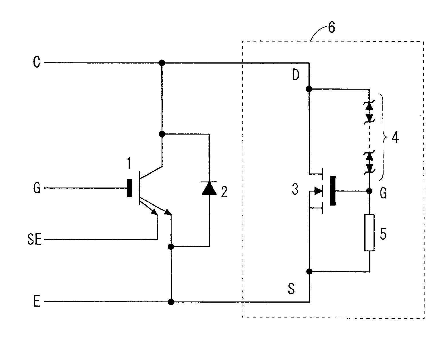
[0029]FIG. 1 shows a circuit diagram of a switching module which is an example of a semiconductor device according to this preferred embodiment. The switching module includes an IGBT 1 which is a main switching element, a recovery diode 2 connected between a collector C and an emitter E of the IGBT 1, and a snubber device 6 which absorbs a surge voltage. The snubber device 6 includes a SiC-MOSFET 3 connected between the collector C and the emitter E of the IGBT 1, a Zener diode 4 connected between a drain D and a gate G of the SiC-MOSFET 3, and a resistor 5 connected between the gate G and a source S of the SiC-MOSFET 3. As the SiC-MOSFET 3, for example, N-channel enhancement-mode one is used. Each of the Zener diode 4 and the resistor 5 is formed of polysilicon.

[0030]A threshold voltage of the Zener diode 4 is normally set higher than a power supply voltage which is applied to the collector of the IGBT 1. When the surge voltage exceeds the threshold voltage of...

embodiment 2

Preferred Embodiment 2

[0039]In the preferred embodiment 1, the Zener diode 4 and the resistor 5 which are necessary for the active clamp are formed on the single chip (snubber device 6) on which the SiC-MOSFET 3 is also formed. While the SiC-MOSFET 3 which absorbs the surge energy is a SiC device operable at a high temperature, the Zener diode 4 and the resistor 5 are formed of polysilicon and therefore their performance is reduced in a high-temperature operation, which causes a bottleneck.

[0040]In a preferred embodiment 2, therefore, the SiC-MOSFET 3 which generates heat in an active clamping operation is formed as an element separate from the Zener diode 4 and the resistor 5 which have no energy load, so that the protection performance against larger surge energy can be exhibited.

[0041]FIG. 5 shows a circuit diagram of a switching module which is an example of a semiconductor device according to the preferred embodiment 2. The same component parts as those of the preferred embodim...

embodiment 3

Preferred Embodiment 3

[0047]In the configuration of the preferred embodiment 2, the special semiconductor device (second snubber device 6b) is required for arranging the Zener diode 4 and the resistor 5 necessary for the active clamping operation. In a preferred embodiment 3, a silicon device is used as the IGBT 1, and the Zener diode 4 and the resistor 5 are formed on a single device (switching device 7) on which the IGBT 1 is also formed. Thereby, the number of chips and the number of wirings are decreased and cost reduction is realized.

[0048]FIG. 9 shows a circuit diagram of a switching module which is an example of a semiconductor device according to the preferred embodiment 3. FIG. 10 is a diagram showing a configuration of the switching module. In FIGS. 9 and 10, the same component parts as those of the preferred embodiment 2 are denoted by the same corresponding reference signs.

[0049]In the switching module, as shown in FIG. 10, the switching device 7, the recovery diode 2, a...


PUM


Abstract

A semiconductor device of the present invention includes a switching transistor, and a recovery diode and a snubber device which are mounted on a single conductive substrate (frame) on which the switching transistor is also mounted. The snubber device includes a SiC-MOSFET connected between an output terminal C and a reference terminal E of the switching transistor, a Zener diode formed between a gate terminal G and a drain terminal D of the SiC-MOSFET, and a resistor formed between the gate terminal G and a source terminal S of the SiC-MOSFET. The reference terminal E of the switching transistor, the source terminal S of the SiC-MOSFET, and an anode terminal of the recovery diode are commonly connected.

Description

BACKGROUND OF THE INVENTION[0001]1. Field of the Invention[0002]The present invention relates to a snubber device which suppresses a surge voltage generated at a time of turn-off of a switching element or a reverse recovery of a diode used in an inverter or a chopper circuit, and also to a semiconductor device using the snubber device.[0003]2. Description of the Background Art[0004]In an inverter semiconductor module using a switching element having a high switching rate, such as an IGBT, a high voltage (turn-off surge voltage) is generated in floating inductance of a main circuit due to a rapid change of a current at a time of turn-off. At a time when a free-wheeling diode is turned off, a surge voltage (recovery surge voltage) is generated on the same principle.[0005]Thereby, an external protection circuit (snubber device) which absorbs such a surge voltage is provided to a semiconductor module, to thereby suppress the surge voltage. In a typical basic configuration of the snubber...

Claims


Application Information

Patent Timeline
Patent Type & Authority Applications(United States)
IPC IPC(8): H02H7/122H02H9/04
CPCH01L23/49575H01L2924/13055H01L28/20H01L29/0619H01L29/1608H01L29/7802H01L29/866H01L2224/48137H01L2224/48247H02M1/34H03K17/08148Y02B70/1483H01L2924/1305H01L2924/30107H01L24/48H01L2924/13091H01L27/0629H01L2924/00H01L2224/48139H01L2924/12035H01L2924/00014H01L24/49H01L2224/05553H01L2224/49111H01L29/7811H01L29/7808Y02B70/10H01L2224/0603H01L2224/45099H01L2224/45015H01L2924/207
Inventor GODO, SHINSUKE
Owner MITSUBISHI ELECTRIC CORP
Why Eureka
Try Eureka